Capacitive sensor

a capacitive sensor and sensor technology, applied in the direction of speed/acceleration/shock measurement, resistance/reactance/impedence, instruments, etc., can solve the problems of generating deficit or sticking of a member, prone to increase and reducing stress generated in the beam. , to achieve the effect of enhancing detection sensitivity, avoiding the movement of a movable electrode, and reducing the size of the devi

Active Publication Date: 2012-05-15
MOSAID TECH
View PDF48 Cites 18 Cited by
  • Summary
  • Abstract
  • Description
  • Claims
  • Application Information

AI Technical Summary

Benefits of technology

[0013]According to the capacitive sensor of the first aspect of the present invention, a portion where a stress is prone to become large in the beam, i.e., at least one of the end connected to the fixed portion of the beam and the end of the beam connected to the movable electrode is provided with the stress moderating unit that moderates a stress. Therefore, a stress generated in the beam can be reduced.
[0014]According to the capacitive sensor of the second aspect of the present invention, it is possible to enhance the detection sensitivity, and a deficit or a sticking of a member generated by increase of device size or movement of a movable electrode can be avoided. By forming the movable mechanism by the vertical etching process, a uniform cross section shape can be obtained and thus, it is possible to largely reduce the sensitivity of the other axis. Further, since the semiconductor layer is the single crystal silicon, there is not film stress, and it is easy to work.

Problems solved by technology

In the case of a structure in which a movable electrode is movable supported by a fixed portion through a beam as in Patent Document 1, a stress generated in the beam is varied depending on a shape of the beam as the elastic element and the maximum acceleration applied to the sensor, but when a thin and long beam is provided when a sensor is made compact or a spring constant is set, a stress generated in the beam is prone to become great, and it becomes difficult to set a specification such as a displacement amount or a weight of the movable electrode to a desired value in some cases.
According to the capacitive sensor disclosed in Patent Document 3, since a single crystal silicon substrate is formed by crystal anisotropy etching, there is a problem that various portions such as an anchor portion are tapered, and a deficit or sticking of a member is generated by increase of device size or movement of a movable electrode.
When the substrate is worked by the crystal anisotropy etching, there is problem that it is difficult to form a mass portion that enhances the detection sensitivity because the mass portion has a mass to some extent.

Method used


Image

  • Capacitive sensor
  • Capacitive sensor
  • Capacitive sensor

Examples


first embodiment

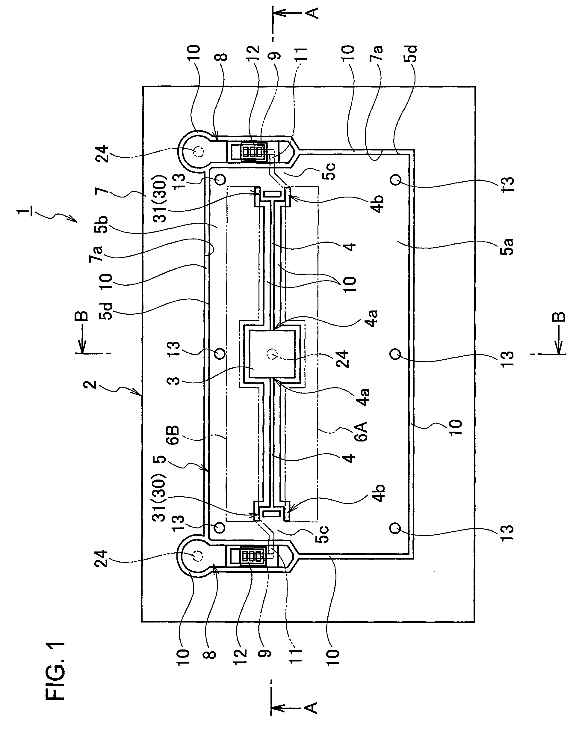
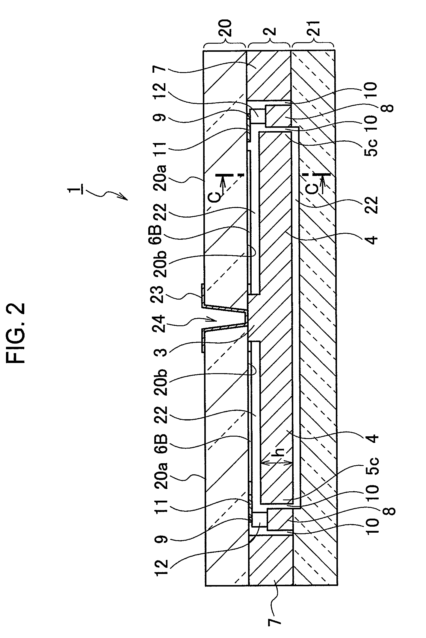
[0036]As shown in FIG. 2, a capacitive sensor 1 (hereinafter, simply sensor 1) as a first embodiment of the present invention has a semiconductor layer 2 obtained by processing a semiconductor substrate, and insulation layers 20 and 21 such as glass substrates are bonded on both front and back sides by anodic bonding. Relatively shallow recesses 22 are formed in bonded surfaces between the semiconductor layer 2 and the insulation layers 20 and 21, insulation properties of the semiconductor layer 2 and moving easiness of the movable electrode 5 are secured. In the present embodiment, the bonded surface between the semiconductor layer 2 and the insulation layer 20 is provided with the recess 22 on the side of the semiconductor layer 2, and the bonded surface between the semiconductor layer 2 and the semiconductor layer 2 is provided with the recess 22 on the side of the insulation layer 21.

[0037]A conductive layer 23 is formed on a surface 20a of the insulation layer 20, and the condu...

second embodiment

[0067]The sensor 1 as a second embodiment of the present invention is different from the structure of the sensor 1 as the first embodiment in that ends of the beam portions 4 and 4 in the longitudinal direction are not provided with the stress moderating units 30 as shown in FIG. 9. In the second embodiment, as shown in FIG. 10(a), the semiconductor layer 2 is bonded to the insulation layer 20, and before the gap 10 is formed, the recess 22 is formed by various etching processes such as wet etching and dry etching. After cutting the semiconductor layer 2 away by the etching, the insulation layer 20 which is a glass substrate is bounded as shown in FIG. 10(b), vertical etching working is carried out, thereby forming the gap 10 as shown in FIG. 10(c). The stopper 13 is formed of oxide film or aluminum alloy after the recess 22 is formed by etching process.

[0068]By etching the semiconductor layer 2 which is the single crystal silicon substrate in this manner, the recess 22 is formed pr...

third embodiment

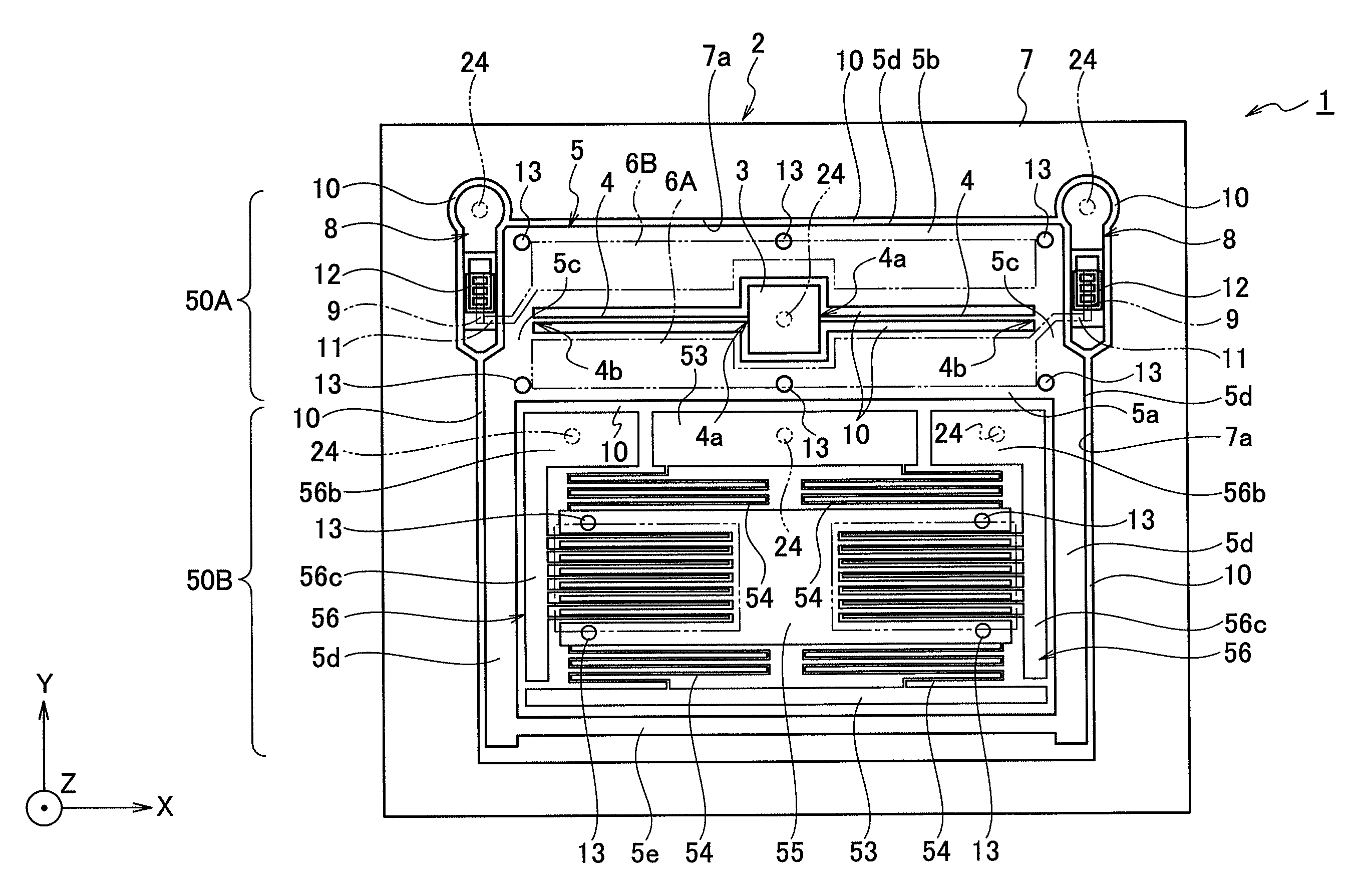
[0092]Next, a structure of the sensor 1 shown as a third embodiment of the present invention will be explained with reference to FIGS. 17 and 18. The sensor 1 shown as the third embodiment is identical to the sensor 1 shown as the second embodiment that detects a physical value in the vertical direction which is the thickness direction of the semiconductor layer 2, except that the sensor 1 shown as the third embodiment can detect a physical value in the horizontal direction which is a plane direction of the semiconductor layer 2.

[0093]FIG. 17 is a plan view showing the semiconductor layer 2 of the sensor 1. As shown in FIG. 17, the semiconductor layer 2 includes a vertical direction detecting unit 50A that detects a physical value in the vertical direction by forming a gap 10 in the semiconductor substrate by a known process, a horizontal direction detecting unit 50B that detects a physical value in the horizontal direction, and a frame portion 7 surrounding these units. Since the v...


PUM


Abstract

A capacitive sensor includes a fixed electrode and a movable electrode that is movably supported by an anchor portion through a beam portion. The fixed electrode and the movable electrode are opposed to each other with a gap interposed therebetween, thereby constituting a detecting unit. A capacitance suitable for a size of the gap is detected to detect a predetermined physical value. At least one of an end of the beam portion connected to the anchor portion and an end of the beam portion connected to the movable electrode is provided with a stress moderating unit that moderates a stress.

Description

TECHNICAL FIELD[0001]The present invention relates to a capacitive sensor that detects a predetermined physical value by detecting a capacitance between a fixed electrode and a movable electrode.BACKGROUND ART[0002]Conventionally, there has been a capacitive sensor in which a structure having a movable electrode supported by a fixed portion through an elastic element is formed, the movable electrode can move toward and away from the fixed electrode according to an external force, and a capacitance between these electrodes is detected, thereby detecting various physical values such as acceleration and angular speed (see Patent Document 1). As such a capacitive sensor, there is also a known capacitive sensor capable of detecting a physical value in a vertical axis direction by one mass portion that is displaced by a physical value such as acceleration (see Patent Document 2 and Patent Document 3).[0003]Patent Document 1: Japanese Patent Application Laid-open No. 2000-28634.[0004]Paten...

Claims


Application Information

Patent Timeline
Patent Type & Authority Patents(United States)
IPC IPC(8): G01P15/125
CPCG01P1/023G01P15/125G01P2015/0831G01R27/26
Inventor FURUKUBO, EIICHIWAKABAYASHI, DAISUKEMIYAJIMA, HISAKAZUOHBUCHI, MASAOAOKI, RYO
Owner MOSAID TECH
Why Eureka
Try Eureka