
N-type carrier enhancement in semiconductors

a technology of n-type carrier and semiconductor, applied in the field of microelectronics, can solve the problems of difficult fabrication of ge nfet, complex technology,

Inactive Publication Date: 2012-05-15
GLOBALFOUNDRIES INC
View PDF24 Cites 114 Cited by
  • Summary
  • Abstract
  • Description
  • Claims
  • Application Information

AI Technical Summary

Problems solved by technology

As FET (Field-Effect-Transistor) devices are being scaled down, the technology becomes more complex, and changes in device structures and new materials are needed for maintaining the expected device performance improvements.
Fabricating a Ge NFET, however, is challenging because of the low attainable n-type carrier concentration in the source and drain.

Method used


Image

  • N-type carrier enhancement in semiconductors
  • N-type carrier enhancement in semiconductors
  • N-type carrier enhancement in semiconductors

Examples


Embodiment Construction

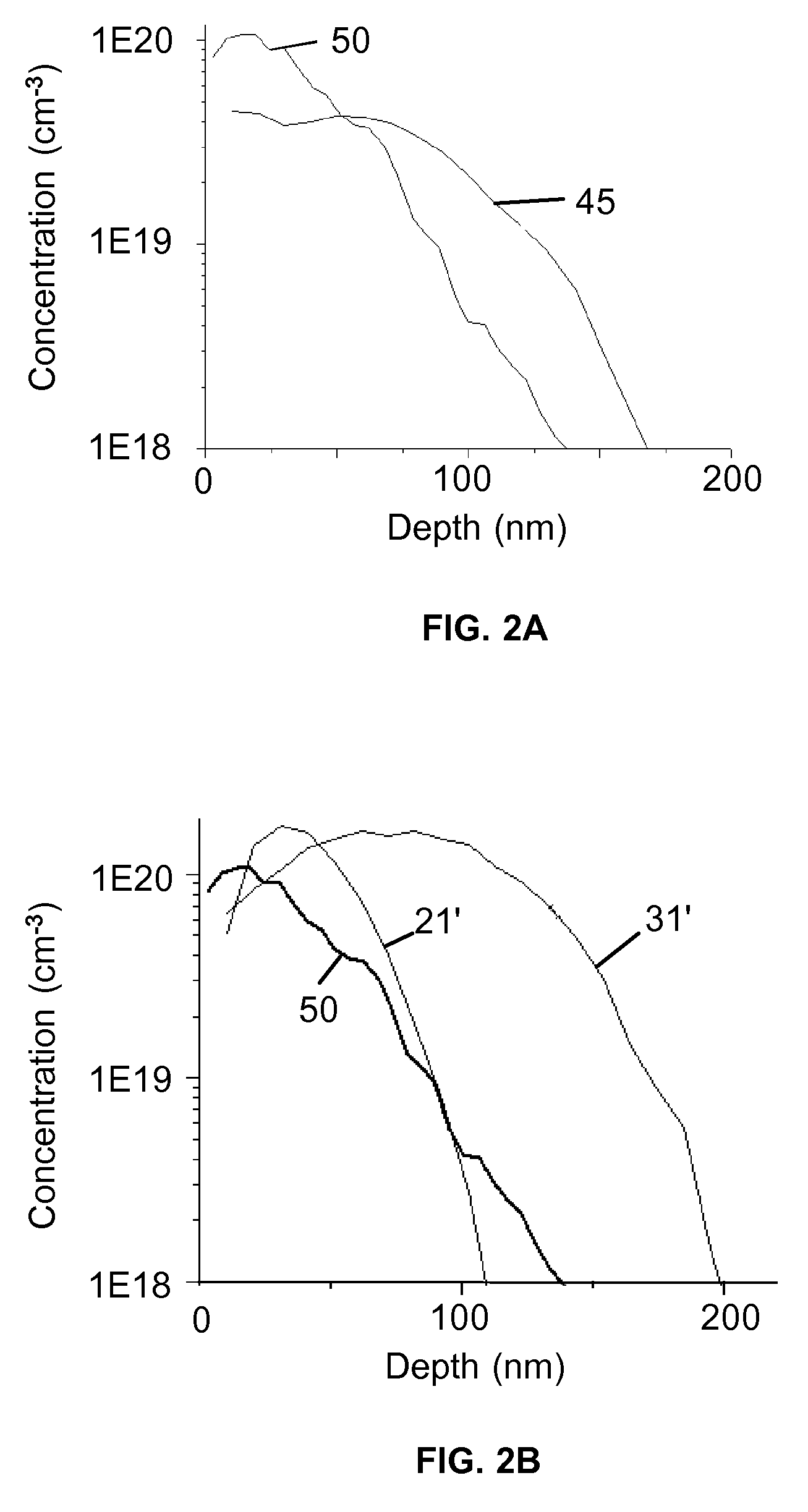
[0014]Germanium (Ge), and silicon germanium (SiGe) with high Ge content, typically over 80%, are strong candidates for maintaining the progress in microelectronics. They may have significantly higher hole and electron mobilities than Si. Embodiments of the present invention enhance the concentration of n-type carrier in Ge and SiGe. The problems to overcome are the relatively low solid solubility limit (SSL) and the poor activation level of n-type dopants, such as phosphorus (P) and arsenic (As), in Ge and in high Ge content SiGe.

[0015]Table 1. shows atomic radius, SSL, and maximum activation level of various elements in Ge.

[0016]

TABLE 1BPAsSb(rB = 0.85 Å)(rP = 1.1 Å)(rAs = 1.21 Å)(rSb = 1.41 Å)Atomic0.340.120.01−0.19radiusdifferencefrom Ge(rGe − rdopant)Equilibrium5.5 × 10182 × 10207.3 × 10191.2 × 1019solubilityin GeActivation1.5 × 1020  4 × 10¹⁹~  2 × 10¹⁹~  8 × 10¹⁸level5 ×10193 ×1019

[0017]For ion-implanted boron (B), using BF2 source as a p-type dopant in germanium, the maximum ...


PUM


Abstract

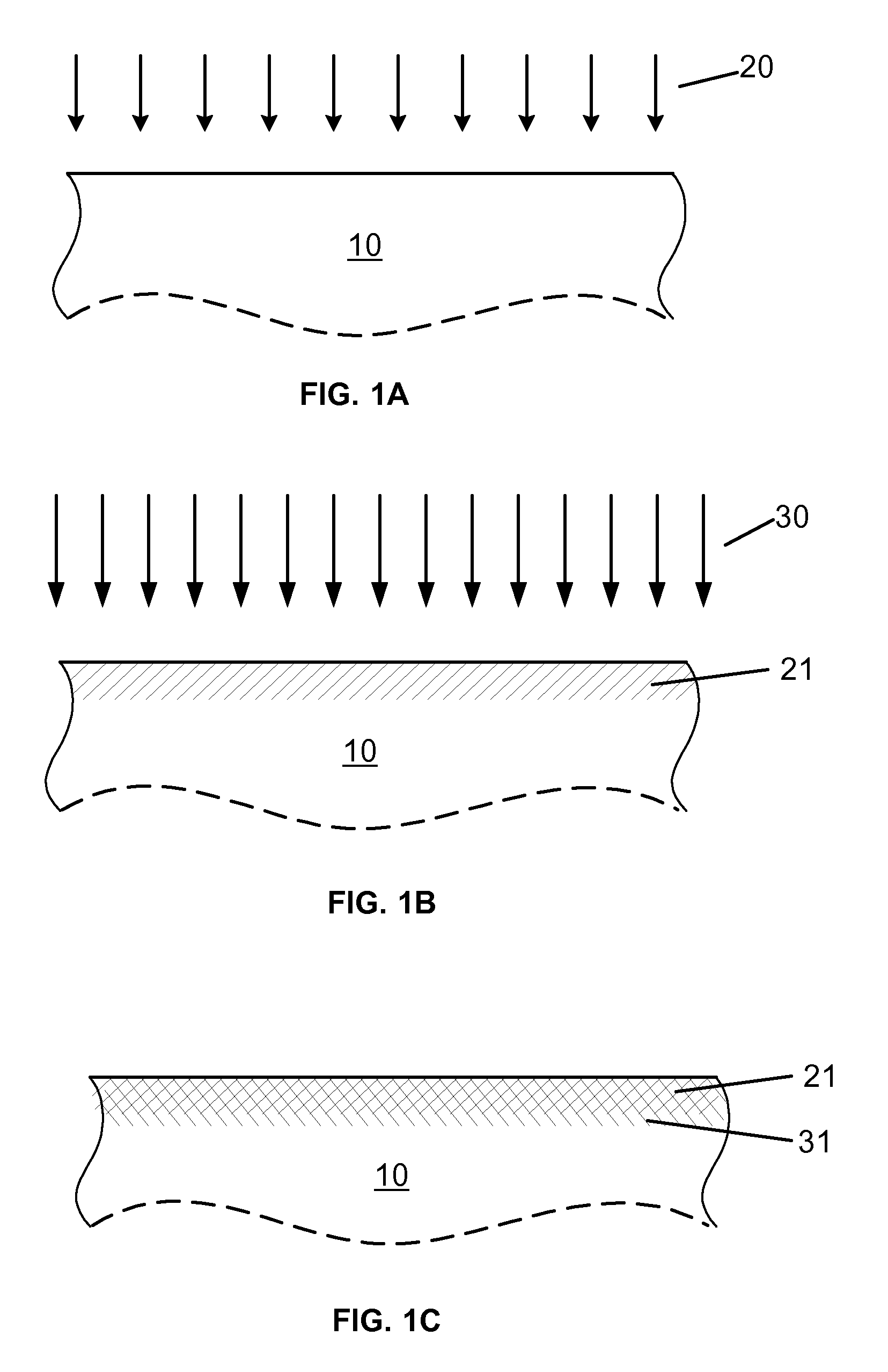
A method for generating n-type carriers in a semiconductor is disclosed. The method includes supplying a semiconductor having an atomic radius. Implanting an n-type dopant species into the semiconductor, which n-type dopant species has a dopant atomic radius. Implanting a compensating species into the semiconductor, which compensating species has a compensating atomic radius. Selecting the n-type dopant species and the compensating species in such manner that the size of the semiconductor atomic radius is inbetween the dopant atomic radius and the compensating atomic radius. A further method is disclosed for generating n-type carriers in germanium (Ge). The method includes setting a target concentration for the carriers, implanting a dose of an n-type dopant species into the Ge, and selecting the dose to correspond to a fraction of the target carrier concentration. Thermal annealing the Ge in such manner as to activate the n-type dopant species and to repair a least a portion of the implantation damage. Repeating the implantation and the thermal annealing until the target n-type carrier concentration has been reached.

Description

FIELD OF THE INVENTION[0001]The present invention relates to microelectronics. In particular, it relates to forming regions of high n-type carrier concentration in semiconductors, especially in germanium.BACKGROUND OF THE INVENTION[0002]Today's integrated circuits include a vast number of devices. Smaller devices and shrinking ground rules are the key to enhance performance and to reduce cost. As FET (Field-Effect-Transistor) devices are being scaled down, the technology becomes more complex, and changes in device structures and new materials are needed for maintaining the expected device performance improvements.[0003]Germanium (Ge) is a strong candidate as a material to replace Si for advanced FET devices. It has significantly higher hole and electron mobilities than Si. Fabricating a Ge NFET, however, is challenging because of the low attainable n-type carrier concentration in the source and drain.SUMMARY OF THE INVENTION[0004]A method is disclosed for generating n-type carriers ...

Claims


Application Information

Patent Timeline
Patent Type & Authority Patents(United States)
IPC IPC(8): H01L21/265H01L21/425
CPCH01L21/26513H01L29/165H01L29/167H01L29/66636Y10S438/919
Inventor KIM, JEE HWANBEDELL, STEPHEN W.MAURER, SIEGFRIEDSADANA, DEVENDRA K.
Owner GLOBALFOUNDRIES INC
Learn More