Component built-in wiring substrate and manufacturing method thereof

a technology of built-in wiring and wiring substrate, which is applied in the direction of fixed capacitor details, fixed capacitors, printed circuit non-printed electric components association, etc., can solve the problems of mounting area swelling, prevent the formation of solder bumps, and suppress swelling in the mounting area.

Active Publication Date: 2012-05-22
NGK SPARK PLUG CO LTD
View PDF7 Cites 35 Cited by
  • Summary
  • Abstract
  • Description
  • Claims
  • Application Information

AI Technical Summary

Benefits of technology

[0011]The present invention has been made in view of the above-described problems. Accordingly a first object of the present invention is to provide a component built-in wiring substrate capable of suppressing swelling in the mounting area for a chip component and preventing formation of a short circuit of the solder bumps. In addition, a second object of the present invention is to provide a method of manufacturing the above-described component built-in wiring substrate.

Problems solved by technology

Thus, as in the conventional technology, when there is a large mismatch in the coefficients of thermal expansion of the core substrate, the plate-shaped component and the resin filling portion, the mounting area swells.

Method used


Image

  • Component built-in wiring substrate and manufacturing method thereof
  • Component built-in wiring substrate and manufacturing method thereof
  • Component built-in wiring substrate and manufacturing method thereof

Examples


Embodiment Construction

[0041]Hereinafter, an embodiment of the present invention will be described in detail with reference to drawings. However, the present invention should not be construed as being limited thereto.

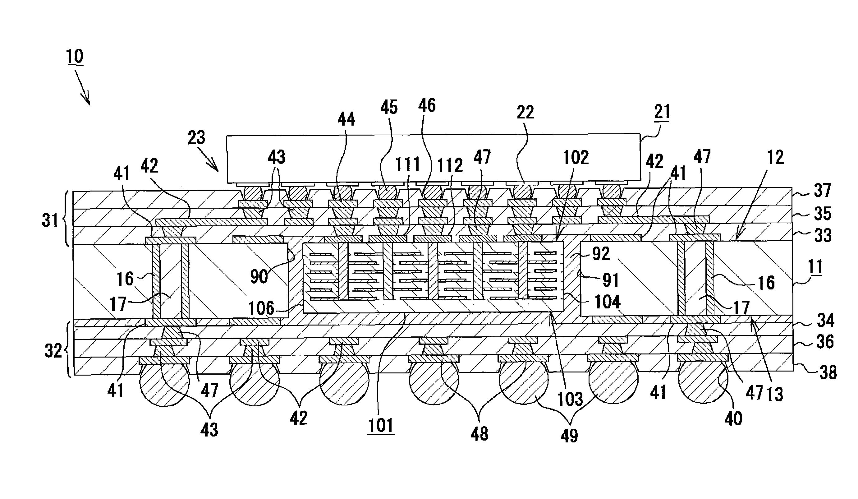
[0042]As shown in FIG. 1, a component built-in wiring substrate 10 according to this embodiment is configured by a core substrate 11 made of a resin, a first buildup layer 31 (wiring stacking portion) that is formed on a core principal surface 12 (a top face in FIG. 1) of the core substrate 11, and a second buildup layer 32 that is formed on a core rear surface 13 (a bottom face in FIG. 1) of the core substrate 11.

[0043]The core substrate 11 has an approximately rectangular plate shape in plan view, which has a vertical length of 25 mm×a horizontal width of 25 mm×a thickness of 1.0 mm. In a plurality of spots located on this core substrate 11, through hole conductors 16 are formed. The through hole conductor 16 allows for electrical connection between the core principal surface 12 side and th...


PUM


Abstract

A component built-in wiring substrate (10) which includes: a core substrate (11); a plate-shaped component (101); a resin filling portion (92); and a wiring stacking portion (31), wherein, when viewed from the core principal surface (12) side, the projected area of the mounting area (32) is larger than the projected area of the plate-shaped component (101) and the resin filling portion, and the plate-shaped component and the resin filling portion are positioned directly below the mounting area (23), and wherein a value of the coefficient of thermal expansion (CTE α2) for a temperature range that is equal to or higher than the glass transition temperature of the resin filling portion is set to be larger than a value of the coefficient of thermal expansion of the plate-shaped component and smaller than a value of the coefficient of thermal expansion of the core substrate for the subject temperature range.

Description

BACKGROUND OF THE INVENTION[0001]1. Field of the Invention[0002]The present invention relates to a component built-in wiring substrate in which a plate-shaped component such as a ceramic capacitor is built and a manufacturing method thereof.[0003]2. Description of the Related Art[0004]Recently, there has been an increase in the speed and level of the function of semiconductor integrated circuit elements (IC chips) that are used as microprocessors of computers and the like. Accompanying such a trend, the number of terminals of the IC chips has been increased, and the pitch between the terminals has been decreased. Generally, on the bottom of the IC chip, a plurality of terminals are densely disposed in an array shape, and such a terminal group is connected to a terminal group of the motherboard side in the form of a flip-chip. However, there is a large difference in the pitch of the terminals between the terminal group of the IC chip side and the terminal group of the motherboard sid...

Claims


Application Information

Patent Timeline
Patent Type & Authority Patents(United States)
IPC IPC(8): H05K1/16
CPCH01L21/4857H01L23/49822H01L23/49827H05K1/0231H05K1/185H01L23/49816H01L2224/16235H01L2224/16225H01L2924/01078H01L2924/09701H01L2924/15312H05K1/113H05K3/4602H05K2201/0187H05K2201/068H05K2201/096H05K2201/10674H05K2201/10712H01L2224/05573H01L2224/05568H01L2924/00014H01L2224/0554H01L2224/05599H01L2224/0555H01L2224/0556H01L23/14
Inventor SUZUKI, SHINYASAITA, KENICHIMIYAMOTO, SHINYAYURI, SHINJI
Owner NGK SPARK PLUG CO LTD
Why Eureka
Try Eureka