Signal processing circuit

a signal processing circuit and circuit technology, applied in the direction of pulse technique, transmission monitoring, line-fault/interference reduction, etc., can solve the problems of almost no hardware to be added for compensation, the above performance requirements are lowered, and the arrangement of the signal processing circuit is prevented from being complex

Active Publication Date: 2012-05-22
NEC CORP
View PDF23 Cites 4 Cited by
  • Summary
  • Abstract
  • Description
  • Claims
  • Application Information

AI Technical Summary

Benefits of technology

[0065]It is an object of the present invention to provide a signal processing circuit which is not of a complex arrangement and which is capable of compensating for an I / Q mismatch of an orthogonal modulator while reducing the effect of a remaining DC offset.
[0067]With the above arrangement, since test signals represented by four points, which comprise two sets of two points positioned in point symmetry with respect to the origin, are generated, and an I / Q mismatch quantity is calculated using the average value of the amplitude of the envelope of the amplitude of the output signal from the orthogonal modulator at the time the test signals represented by the two points of each set are generated, the effect of a remaining DC offset is removed.
[0068]Furthermore, inasmuch as test signals represented by four points, which comprise two sets of two points positioned in point symmetry with respect to the origin, are used, the test signals may be simplified as being of a rectangular wave. Accordingly, no means for generating sine-wave test signals may be required, and a memory area for storing the test signals may be small. As a result, the arrangement of the signal processing circuit is prevented from being complex.

Problems solved by technology

As the rate of communications has become higher in recent years, however, the above performance requirements, though they have been required to be met at higher levels, tend to be lowered due to circuit limitations posed by a direct conversion architecture and a lower process voltage.
However, it is ideal for nearly no hardware to be added for compensation.
However, the background art described above has the following problems:
However, Patent document 1 discloses only a method of compensating for an I / Q phase mismatch, but not a method of compensating for an I / Q amplitude mismatch.
However, the orthogonal modulator necessarily suffers an input-converted DC offset because of the problem of its manufacturing accuracy.
Nevertheless, using the method disclosed in Patent document 1 requires a DC offset to be removed with much higher accuracy than the amount of the DC offset allowed by the wireless communication system, bringing about packaging complexities.
The background art disclosed in Patent document 2 is problematic in that it requires a complex system including a test signal generator for generating sine-wave test signals and an ND converter.
The background art disclosed in Patent document 3 is problematic in that it requires a complex system and, additionally, the I / Q accuracy of an I / Q orthogonal downconverter used for a compensating process is responsible for an error of the compensating process.
However, a compensating process is performed because an orthogonal modulator having a high modulating accuracy is not practically available, and it is contradictory to require an I / Q orthogonal downconverter having a high I / Q accuracy as a means for such a compensating process.
The background art disclosed in Patent documents 4, 5 is also problematic in that it requires a complex system including a test signal generator and an A / D converter.
However, no means for solving the problems is disclosed in Patent documents 4, 5.
Consequently, a piece of hardware needs to be added for solving the four simultaneous equations, and the accuracy of the compensating quantities is low.
The background art disclosed in Patent documents 8, 9 is problematic in that the accuracy of an orthogonal demodulator which is used as a detecting system in an operation to compensate for an I / Q phase mismatch and an I / Q amplitude mismatch is responsible for an error of the compensating process.
However, a compensating process is performed because an orthogonal modulator having a high modulating accuracy is not practically available, and it is contradictory to require an orthogonal demodulator having a high I / Q accuracy as a means for such a compensating process.
In an operation to compensate for an I / Q phase mismatch, if a DC offset remains in an orthogonal demodulator, then since the DC offset is reflected as an offset of a compensation quantity for correcting a transmission baseband signal, it leads to an increase a carriage leak of the orthogonal modulator.

Method used


Image

  • Signal processing circuit
  • Signal processing circuit
  • Signal processing circuit

Examples


1st exemplary embodiment

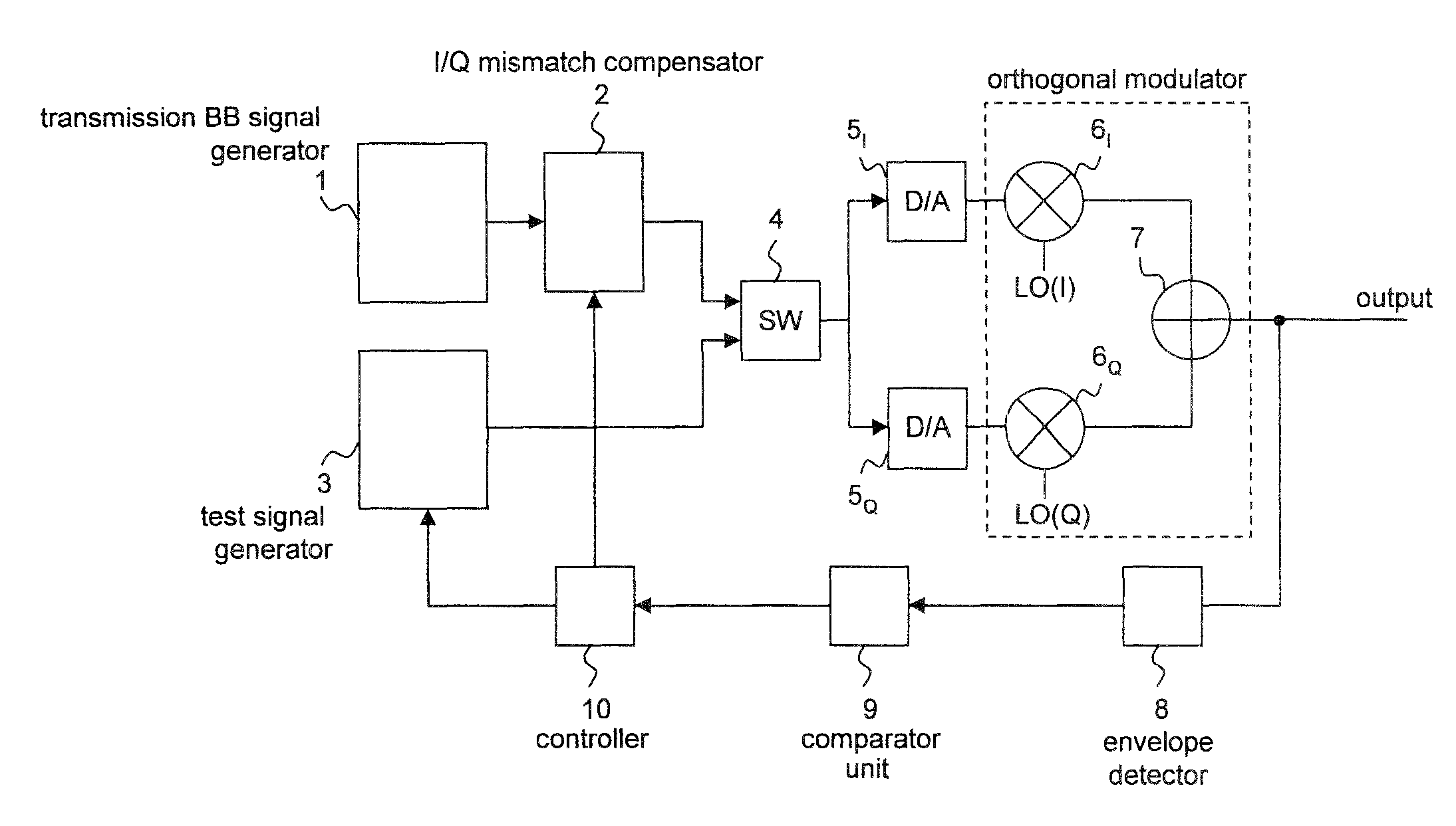
[0105]FIG. 9 is a block diagram showing the overall arrangement of a signal processing circuit according to a first exemplary embodiment of the present invention.

[0106]As shown in FIG. 9, the signal processing circuit according to the present exemplary embodiment comprises transmission BB (BaseBand) signal generator 1, I / Q mismatch compensator 2, test signal generator 3, switch 4, D / A converters 5I, 5Q, mixers 6I, 6Q, adder 7, envelope detector 8, comparator unit 9, and controller 10.

[0107]Transmission BB signal generator 1 generates a transmission baseband signal in a transmitting process.

[0108]In a compensating process, a compensation quantity for compensating for an I / Q mismatch of an orthogonal modulator is set in I / Q mismatch compensator 2 by controller 10. In the transmitting process, I / Q mismatch compensator 2 corrects the transmission baseband signal generated by transmission BB signal generator 1 based on the compensation quantity set by controller 10.

[0109]In the compensat...


PUM


Abstract

Test signal generator (3) generates test signals represented, by four points, which comprise two sets of two points positioned in point symmetry with respect to the origin of an I / Q orthogonal coordinate system. Envelope detector (8) detects the amplitude of an envelope of the output signal from an orthogonal modulator when the test signals represented by four points are generated, and outputs a signal proportional to the square of the amplitude. Comparing unit (9) calculates an average value of output signals from envelope detector ( ) when the test signals represented by the two points of each set are generated. Controller (10) adjusts the amplitudes and / or phases of the test signals so that the average values produced when the test signals represented by the two sets of the two points are generated are equal to each other, and calculates an I / Q mismatch quantity based on the adjusted results.

Description

TECHNICAL FIELD[0001]The present invention relates to a signal processing circuit in a transmission apparatus for orthogonally modulating a transmission baseband signal including an I (in-phase) component and a Q (quadrature) component, and more particularly to a technology for improving the modulation accuracy of orthogonal modulation.BACKGROUND ART[0002]In signal processing circuits of the type described above, it is indispensable performance requirements to suppress a carrier leak and prevent the modulation accuracy from being lowered in orthogonal modulators for achieving communication quality and complying with rules and regulations.[0003]The carrier leak corresponds a DC offset of I / O components as converted into an input to the orthogonal modulator. Factors that affect the modulation accuracy of the orthogonal modulator include a variation (a factor responsible for an I / Q mismatch to be described later) in the levels of I / O components as converted into an input to the orthogo...

Claims


Application Information

Patent Timeline
Patent Type & Authority Patents(United States)
IPC IPC(8): H03C3/00
CPCH04L27/364
Inventor MATSUNO, NORIAKIYANAGISAWA, KIYOSHI
Owner NEC CORP
Why Eureka
Try Eureka