Preparation method of SOI-based concave gate enhanced GaN power switch device

A power switching device, enhanced technology, applied in semiconductor/solid-state device manufacturing, electric solid-state devices, semiconductor devices, etc., can solve problems such as lattice mismatch and thermal mismatch, and achieve low gate leakage current and breakdown voltage The effect of improving and suppressing the current collapse phenomenon

Active Publication Date: 2020-10-02
SHANGHAI INST OF MICROSYSTEM & INFORMATION TECH CHINESE ACAD OF SCI
View PDF5 Cites 1 Cited by
  • Summary
  • Abstract
  • Description
  • Claims
  • Application Information

AI Technical Summary

Problems solved by technology

[0007] The technical problem to be solved by the present invention is to provide a method for preparing a SOI-based recessed gate enhanced GaN power switching device, so as to overcome the lattice mismatch and thermal mismatch between the substrate and GaN in the GaN HEMT device material in the prior art. matching problem

Method used


Image

  • Preparation method of SOI-based concave gate enhanced GaN power switch device
  • Preparation method of SOI-based concave gate enhanced GaN power switch device
  • Preparation method of SOI-based concave gate enhanced GaN power switch device

Examples


Embodiment 1

[0049] This embodiment provides a method for fabricating an SOI-based concave gate enhanced GaN power switching device, and the specific steps are as follows:

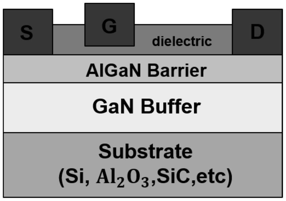
[0050] (1) if image 3 As shown, 100nmSi was deposited on the surface of SOI-based GaN epitaxial layer by LPCVD technology 3 N 4 As the first passivation layer, the SOI-based epitaxial layer includes from bottom to top: Si(100), SiO 2 , Si(111), GaN (including transition layer and channel layer), AlGaN, GaN cap layer;

[0051] (2) if Figure 4 As shown, the photoresist is spin-coated, and the photolithography is developed to determine the source and drain regions. After development, RIE technology is used to etch the Si in the source and drain regions. 3 N 4 , the etching atmosphere is SF 6 、C 4 f 8 Wait. Then use the magnetron sputtering method to grow Ti(20nm) / Al(100nm) / Ti(20nm) / TiN(60nm) metal stacks as the source and drain metal, use the lift-off method to strip off the remaining metal and then anneal to f...

Embodiment 2

[0061] This embodiment provides a method for fabricating an SOI-based concave gate enhanced GaN power switching device, and the specific steps are as follows:

[0062] (1) if image 3 As shown, 100nmSi was deposited on the surface of SOI-based GaN epitaxial layer by LPCVD technology 3 N 4 As the first passivation layer, the SOI-based epitaxial layer includes from bottom to top: Si(100), SiO 2 , Si(111), GaN (including transition layer and channel layer), AlGaN, GaN cap layer;

[0063] (2) if Figure 4 As shown, the photoresist is spin-coated, and the photolithography is developed to determine the source and drain regions. After development, RIE technology is used to etch the Si in the source and drain regions. 3 N 4 , the etching atmosphere is SF 6 、C 4 f 8 Wait. Then use the magnetron sputtering method to grow Ti(20nm) / Al(100nm) / W(60nm) metal stack as the source and drain metal, use the lift-off method to strip off the remaining metal and then anneal to form an ohmic...

Embodiment 3

[0073] This embodiment provides a method for fabricating an SOI-based concave gate enhanced GaN power switching device, and the specific steps are as follows:

[0074] (1) if image 3 As shown, 100nmSi was deposited on the surface of SOI-based GaN epitaxial layer by LPCVD technology 3 N 4 As the first passivation layer, the SOI-based epitaxial layer includes from bottom to top: Si(100), SiO 2 , Si(111), GaN (including transition layer and channel layer), AlGaN, GaN cap layer;

[0075] (2) if Figure 4 As shown, the photoresist is spin-coated, and the photolithography is developed to determine the source and drain regions. After development, RIE technology is used to etch the Si in the source and drain regions. 3 N 4 , the etching atmosphere is SF 6 、C 4 f 8 Wait. Then use the magnetron sputtering method to grow Ti(20nm) / Al(100nm) / Ti(20nm) / TiN(60nm) metal stacks as the source and drain metal, use the lift-off method to strip off the remaining metal and then anneal to f...


PUM


Abstract

The invention relates to a preparation method of an SOI-based concave gate enhanced GaN power switch device. The preparation method comprises the following steps of passivating for the first time; forming the ohmic contact in the source and drain regions; carrying out ion implantation; etching a concave gate region; growing a gate dielectric layer and a gate metal; passivating for the second time;opening a source-drain window; performing deep groove etching for the first time; performing deep groove etching for the second time. The advantages of simpler process and small gate leakage currentbrought by a concave gate structure prepared by the method and the device monolithic isolation advantage brought by an SOI material lay a solid foundation for realizing a GaN monolithic integrated half-bridge circuit, and a new direction for the development of GaN power devices is provided.

Description

technical field [0001] The invention belongs to the field of power devices, and in particular relates to a preparation method of an SOI-based recessed gate enhanced GaN power switch device. Background technique [0002] The arrival of the post-Moore era and the 5G era calls for semiconductor materials with superior performance. Compared with traditional semiconductor materials such as silicon, GaN, a wide bandgap semiconductor, has many advantages such as large bandgap width, high breakdown electric field, large thermal conductivity, and high electron saturation speed. Therefore, GaN power devices have low on-resistance, high switching efficiency, and low cost. It has the characteristics of low leakage current and is very suitable for making high-power devices with high temperature resistance and high frequency. It can be expected that GaN power semiconductors will be widely used in microwave radio frequency fields (such as 5G, radar) and high-power power electronics fields...

Claims


Application Information

Patent Timeline
IPC IPC(8): H01L21/335H01L29/778H01L29/423H01L27/12
CPCH01L27/1203H01L29/4236H01L29/66462H01L29/7787
Inventor 郑理游晋豪程新红俞跃辉
Owner SHANGHAI INST OF MICROSYSTEM & INFORMATION TECH CHINESE ACAD OF SCI
Why Eureka
Try Eureka