Methods and systems for computer aided design of 3D integrated circuits

a computer-aided design and integrated circuit technology, applied in cad circuit design, program control, instruments, etc., can solve the problems of relatively few designers having the opportunity to develop 3-d integrated circuits for fabrication, unable to allow design rule checks or netlist extraction

Active Publication Date: 2012-06-26
R3 LOGIC
View PDF16 Cites 144 Cited by
  • Summary
  • Abstract
  • Description
  • Claims
  • Application Information

AI Technical Summary

Problems solved by technology

Because technologies for fabricating 3-D integrated circuits have not yet become firmly established, relatively few designers have had the opportunity to develop 3-D circuits for fabrication.
This method does not allow design rule checks or netlist extraction, however.
It also results in multiple replications of the electrical and physical design rules for each design layer and is very inefficient in terms of memory usage.
The text, Three-Dimensional Integrated Circuit Layout (Distinguished Dissertations in Computer Science), by Harter, A. C., Cambridge University Press, November, 1991, describes some primitive methods for creating topologies for wiring standard cells on multiple layers, but does not provide direct methods for efficiently creating the mask artwork.

Method used


Image

  • Methods and systems for computer aided design of 3D integrated circuits
  • Methods and systems for computer aided design of 3D integrated circuits
  • Methods and systems for computer aided design of 3D integrated circuits

Examples


Embodiment Construction

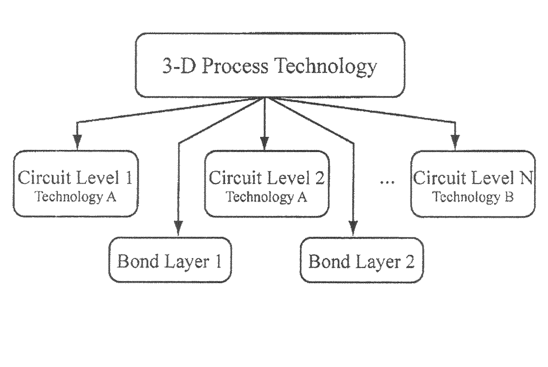
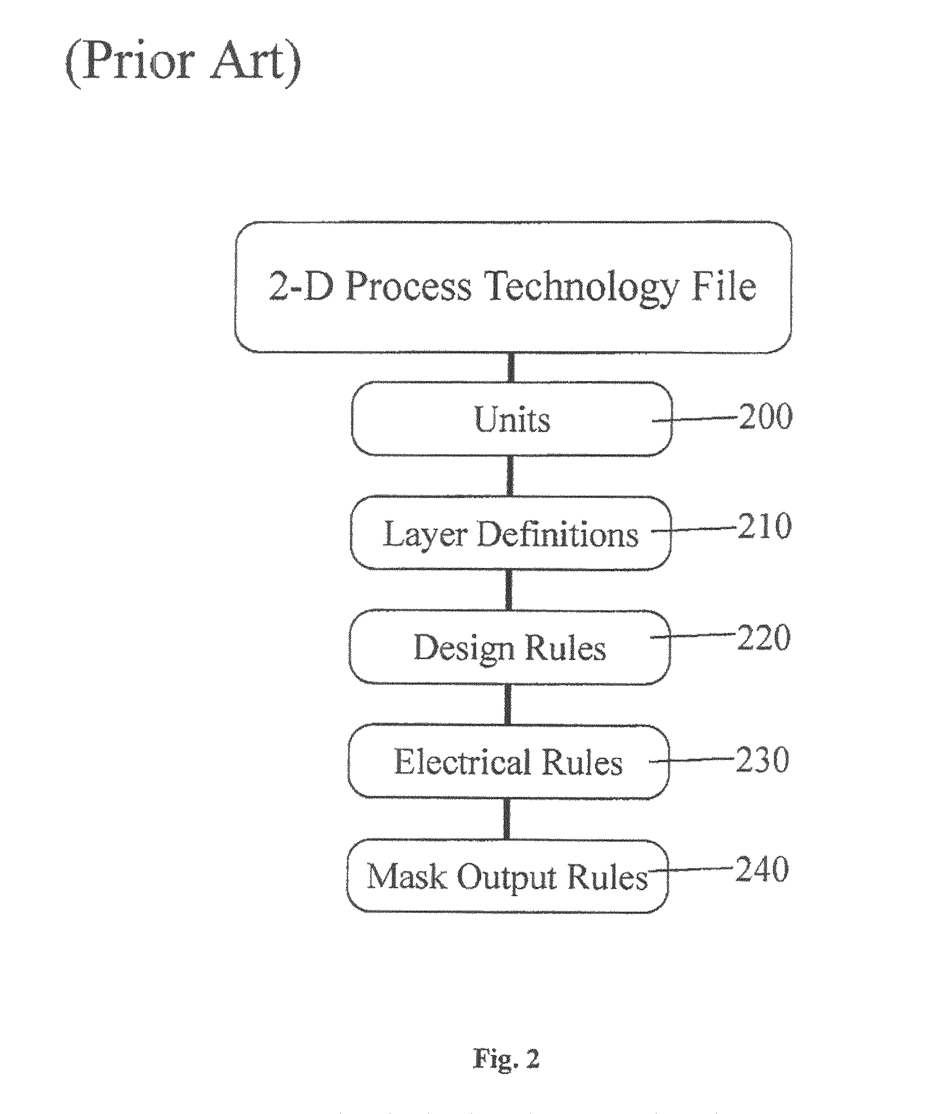
[0048]Methods and systems for generating and verifying circuit layouts from computer-aided design tools for vertically integrated, three-dimensional integrated circuits are disclosed herein below.

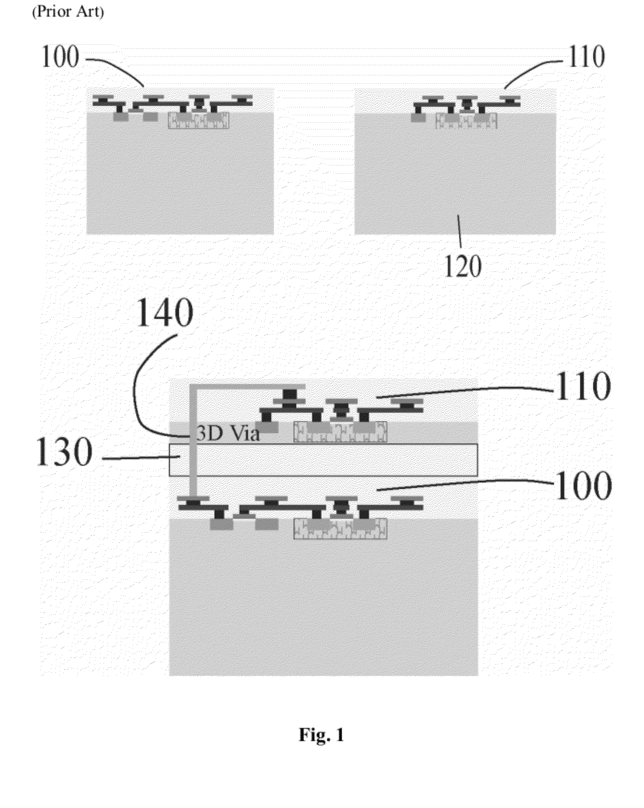
[0049]A three-dimensional, or 3-D, integrated circuit is one comprising multiple levels of semiconductor substrates, each containing active devices therein, in which the different substrates are vertically stacked and electrical interconnections may be made between circuit components on different levels. A significant innovation of emerging 3-D integration technology is that the vertical interconnections may be placed anywhere within the area of any circuit level. This feature provides for a tremendous improvement in device density, but it also adds new constraints for the designer, who should ensure that appropriate design rules are met and that the 3-D physical circuit will function according to the specifications of the logic design.

[0050]The ability to provide arbitrarily placed vertica...


PUM


Abstract

Methods and systems for generating and verifying circuit layouts from computer-aided design tools for vertically integrated, three-dimensional integrated circuits are disclosed. In one instance, a 3-D technology file of these teachings is obtained by providing an identifier for two or more circuit levels, providing for each one of the two or more circuit levels an identifier for a 2-D technology file corresponding to each of the one or more circuit levels and providing a file structure including the two or more circuit levels and each identifier, corresponding to each one of the one or more circuit levels, for the 2-D technology file corresponding to each one of the two or more circuit levels. Other embodiments are disclosed.

Description

CROSS REFERENCE TO RELATED APPLICATIONS[0001]This application is a continuation of U.S. patent application Ser. No. 12 / 233,260, filed Sep. 18, 2008 which is a divisional of U.S. patent application Ser. No. 11 / 485,883 filed Jul. 13, 2006, which, in turn, claims priority to U.S. Provisional Application 60 / 702,364 entitled “METHODS AND SYSTEMS FOR COMPUTER AIDED DESIGN OF 3D INTEGRATED CIRCUITS,” filed on Jul. 26, 2005, all of which are incorporated by reference herein in their entirety.STATEMENT REGARDING FEDERALLY SPONSORED RESEARCH OR DEVELOPMENT[0002]This invention was made partially with U.S. Government support from the Defense Advanced Research Projects Agency under Contract No. DAAH01-03-C-R167. The U.S. Government has certain rights in the invention.BACKGROUND OF THE INVENTION[0003]Ever since the planar integrated circuit was invented independently by Robert Noyce and Jack Kilby in 1959, designers have sought methods to automate the process of creating the mask artwork necessar...

Claims


Application Information

Patent Timeline
Patent Type & Authority Patents(United States)
IPC IPC(8): G06F17/50
CPCG06F17/5045G06F17/5068G06F17/5081G06F30/39G06F30/30G06F30/398
Inventor MCILRATH, LISA G.
Owner R3 LOGIC
Why Eureka
Try Eureka