Reverse-conducting semiconductor device

a reverse-conducting, semiconductor technology, applied in the direction of semiconductor devices, electrical equipment, transistors, etc., can solve the problems of generating losses for igbt and diodes

Active Publication Date: 2012-07-03
HITACHI ENERGY LTD
View PDF6 Cites 42 Cited by
  • Summary
  • Abstract
  • Description
  • Claims
  • Application Information

AI Technical Summary

Problems solved by technology

However, both the IGBT and diode are generating losses.

Method used


Image

  • Reverse-conducting semiconductor device
  • Reverse-conducting semiconductor device
  • Reverse-conducting semiconductor device

Examples


Embodiment Construction

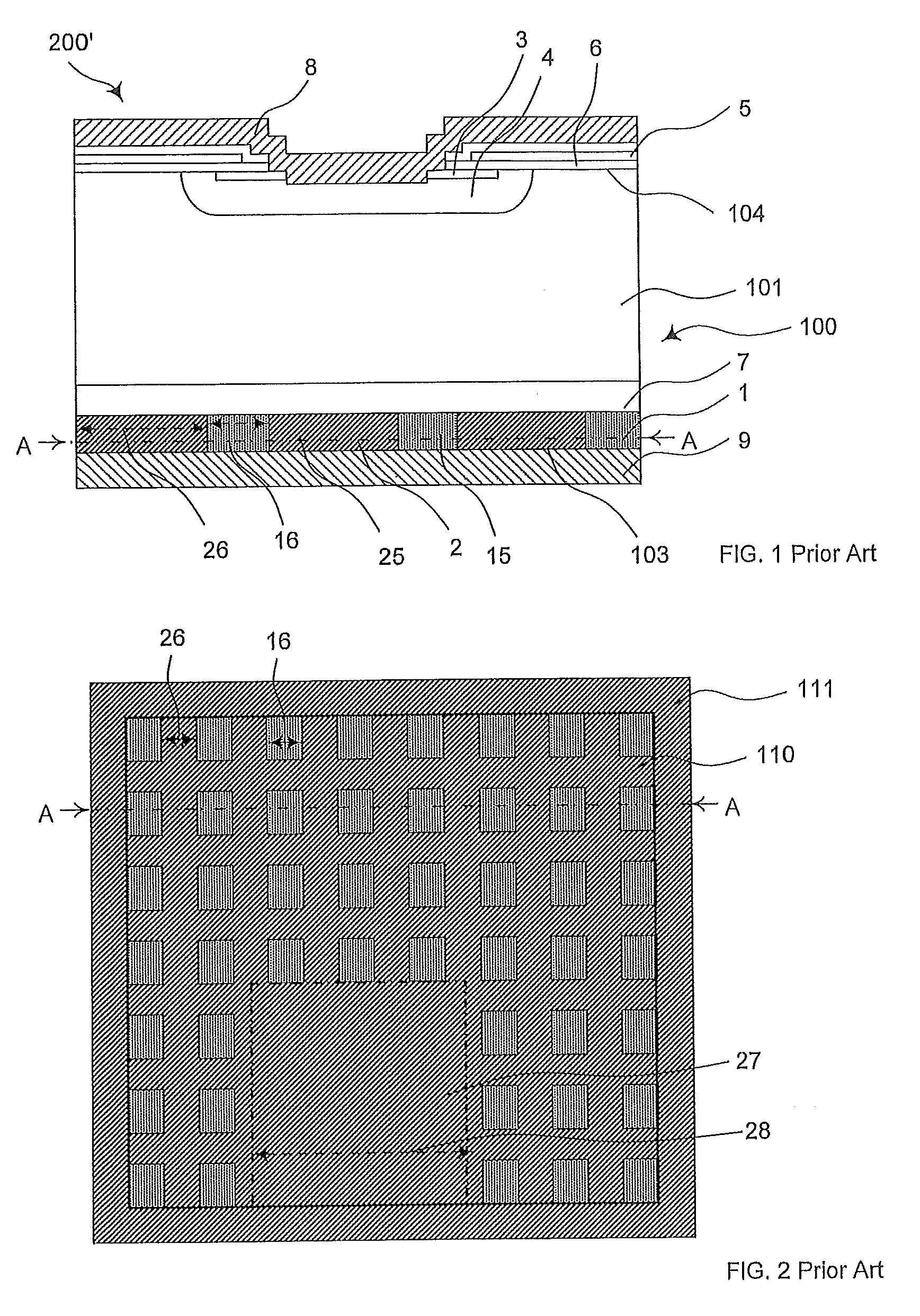
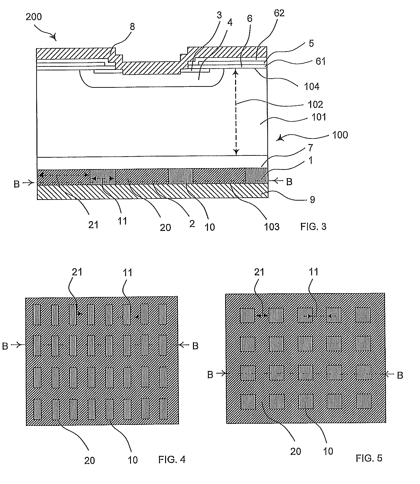
[0029]A reverse-conducting semiconductor device is disclosed which can possess improved electrical and thermal properties relative to known devices.

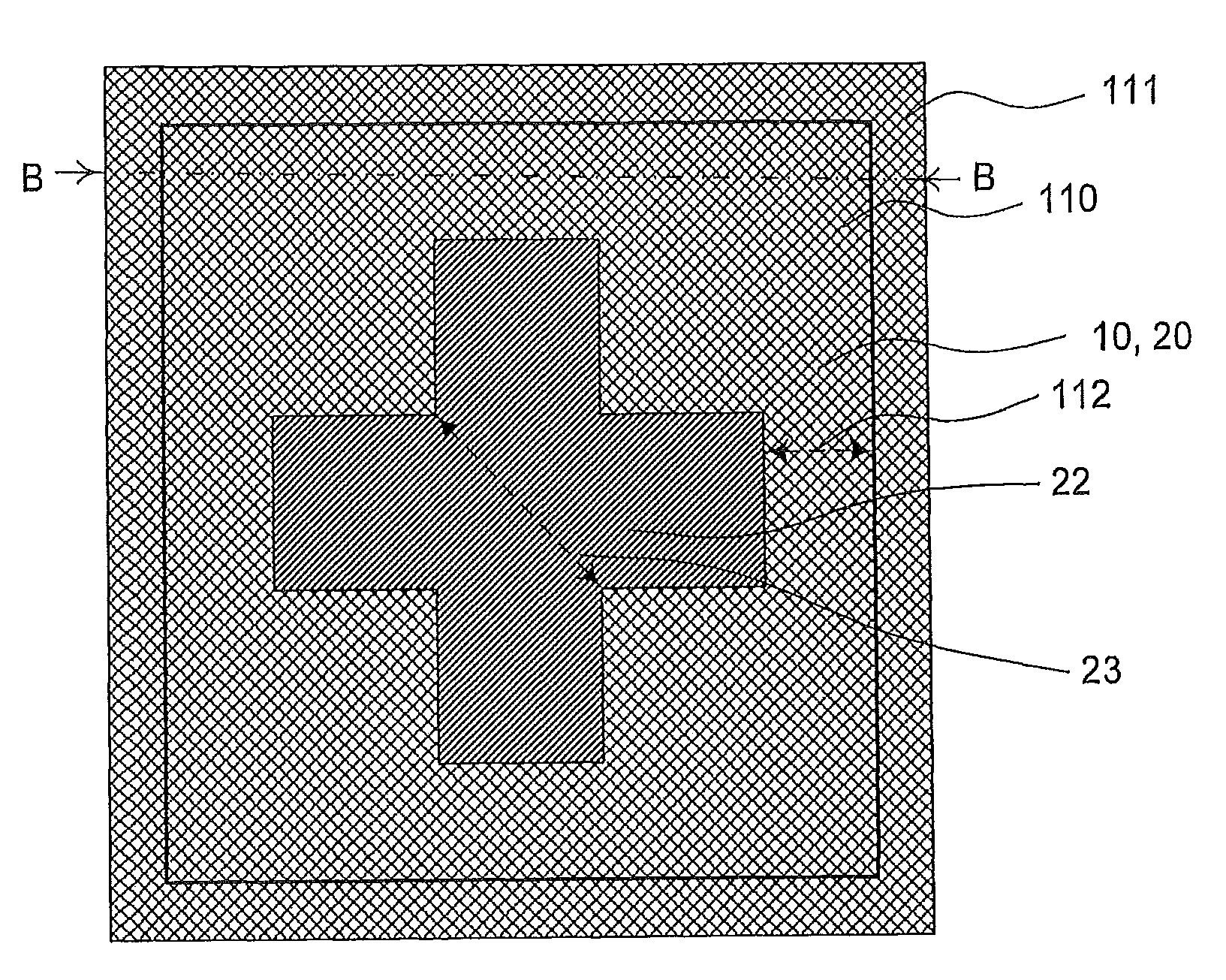
[0030]An exemplary reverse-conducting insulated gate bipolar transistor (RC-IGBT) as disclosed herein includes a freewheeling diode and an insulated gate bipolar transistor (IGBT) on a common wafer, part of which wafer forms a base layer of a first conductivity type with a first doping concentration and a base layer thickness. The insulated gate bipolar transistor includes a collector side and an emitter side, whereas the collector side is arranged opposite of the emitter side of the wafer.

[0031]The base layer thickness is, for example, a maximum vertical distance between the collector and emitter side of that part of the wafer with the first doping concentration.

[0032]A first layer of the first conductivity type and higher doping concentration than the first doping concentration and a second layer of a second conductivity type can be al...


PUM


Abstract

A reverse-conducting semiconductor device is disclosed with an electrically active region, which includes a freewheeling diode and an insulated gate bipolar transistor on a common wafer. Part of the wafer forms a base layer with a base layer thickness. A first layer of a first conductivity type with at least one first region and a second layer of a second conductivity type with at least one second and third region are alternately arranged on the collector side. Each region has a region area with a region width surrounded by a region border. The RC-IGBT can be configured such that the following exemplary geometrical rules are fulfilled: each third region area is an area, in which any two first regions have a distance bigger (i.e., larger) than two times the base layer thickness; the at least one second region is that part of the second layer, which is not the at least one third region; the at least one third region is arranged in the central part of the active region in such a way that there is a minimum distance between the third region border to the active region border of at least once the base layer thickness; the sum of the areas of the at least one third region is between 10 and 30% of the active region; and each first region width is smaller than the base layer thickness.

Description

RELATED APPLICATIONS[0001]This application claims priority under 35 U.S.C. §119 to European Patent Application No. 09159009.1 filed in Europe on Apr. 29, 2009 and European Patent Application No. 10154064.9 filed in Europe on Feb. 19, 2010, the entire contents of these applications being hereby incorporated by reference in their entireties.FIELD[0002]The disclosure relates to the field of power electronics, such as reverse-conducting semiconductor devices.BACKGROUND INFORMATION[0003]US 2008 / 0135871 A1 discloses a reverse-conducting semiconductor device 200′ such as a reverse-conducting insulated gate bipolar transistor (RC-IGBT) as shown in FIG. 1. The device 200′ shown in FIG. 1 includes, within one wafer 100, an insulated gate bipolar transistor with a built-in freewheeling diode. As shown in FIG. 1, such a reverse-conducting semiconductor device 200′ includes an n type base layer 101 with a first main side, which is the emitter side 104 of the integrated IGBT, and a second main si...

Claims


Application Information

Patent Timeline
Patent Type & Authority Patents(United States)
IPC IPC(8): H01L29/739
CPCH01L29/0834H01L29/7395H01L29/66333H01L29/7397
Inventor STORASTA, LIUTAURASRAHIMO, MUNAFVON ARX, CHRISTOPHKOPTA, ARNOSTSCHNELL, RAFFAEL
Owner HITACHI ENERGY LTD
Why Eureka
Try Eureka