Nanopin manufacturing method and nanometer sized tip array by utilizing the method

a nano-tip array and nano-pin technology, applied in the field of nano-pin manufacturing methods, can solve the problems of difficult to increase the brightness use a large amount of chemical reagents, and only 10% of the transmittance of liquid crystal displays, etc., to achieve the effect of low cost, low cost and easy modification of the aspect ratio and the density of fabricated nano-pins

Inactive Publication Date: 2012-07-10
NAT TAIWAN UNIV OF SCI & TECH
View PDF4 Cites 0 Cited by
  • Summary
  • Abstract
  • Description
  • Claims
  • Application Information

AI Technical Summary

Benefits of technology

[0007]In accordance with an aspect of the present invention, utilizing a crystal anisotropic hardness property, nanopins are fabricated on a foil by ion beam dry etching. The aspect ratio and the density of the fabricated nanopins can be altered by adjusting the energy and the current density of ion beam. A capillaritron plasma source is the most important device required for the present invention. No chemical reagents will be needed. The nanopin manufacturing method according to the present invention has an advantage of low cost, and is harmless to the environment. The foil employed can be a zinc foil, a tungsten foil, or a tantalum foil. If a zinc foil is utilized to fabricate zinc nanopins, the nanopin end radius of less than 10 nm and an aspect ration between 25 to 30 can be achieved. The field emission measurement of the zinc nanopins indicates that electrons emits at a threshold field of 12.5 V / μm and a current density of 17 mA / cm2 is achieved at an applied field of 14 V / μm.
[0008]According to the present invention, by controlling the temperature of the foil, cone-shaped nanostructures with various tip angles can be achieved. The higher the temperature of the foil is, the smaller the obtained tip angle and the greater the aspect ratio will be. If the foil is a zinc foil, then zinc nanopins with tip angles smaller than 3 degrees can be fabricated. The tip angles of the zinc nanopins can be controlled by altering the temperature of the zinc foil. By doing so, the threshold field applied to the zinc nanopins to emit electrons can be reduced.
[0009]In accordance with another aspect of the present invention, by ion beam implantation and thermal oxidation, metal oxide nanopins are fabricated on a metal foil polished with an ion beam. The present invention proposes two kinds of ion beam implantation, oxygen ion beam implantation and nitrogen ion beam implantation. Other kinds of ion beam implantation can be utilized as well. For an array of zinc oxide (ZnO) nanopins, before and after oxygen ion beam implantation, the field emission measurement of the ZnO nanopins indicates that the threshold field to emit electrons is reduced from 9.0 V / μm to 6.5 V / μm. In addition, when an electric field of 10 V / μm is applied, the current density of emitted electrons is increased from 20 μA / cm2 to 170 μA / cm2. The density of the ZnO nanopins and the field emission properties of the ZnO nanopins can be improved by nitrogen ion beam implantation. However, the field emission properties of the ZnO nanopins obtained by utilizing oxygen ion beam implantation is superior to that utilizing nitrogen ion beam implantation.
[0010]The metal and metal oxide nanopin manufacturing method provided by the prevent invention is harmless to the environment. The present invention does not use chemical reagents in the nanopin manufacturing process. In addition, the capillaritron plasma source utilized in the present invention is simple in structure and the manufacturing process is not complicated and time-consuming. Moreover, the nanopins fabricated according to the present invention, for example, Zn nanopins and ZnO nanopins, are good in quality and are quite suitable for applying to field emission arrays.

Problems solved by technology

However, the transmittance of liquid crystal display is only 10%.
This is the reason why it is difficult to increase the brightness of liquid crystal display.
However, it is necessary to use a great amount of chemical reagents for growing desired nanotip structures at high temperature.
These chemical reagents may cause pollution or damage to the environment.
In addition, the processes to manufacture the three kinds of field emitter arrays are complicated, and a lot of time would be needed.

Method used


Image

  • Nanopin manufacturing method and nanometer sized tip array by utilizing the method
  • Nanopin manufacturing method and nanometer sized tip array by utilizing the method
  • Nanopin manufacturing method and nanometer sized tip array by utilizing the method

Examples


Embodiment Construction

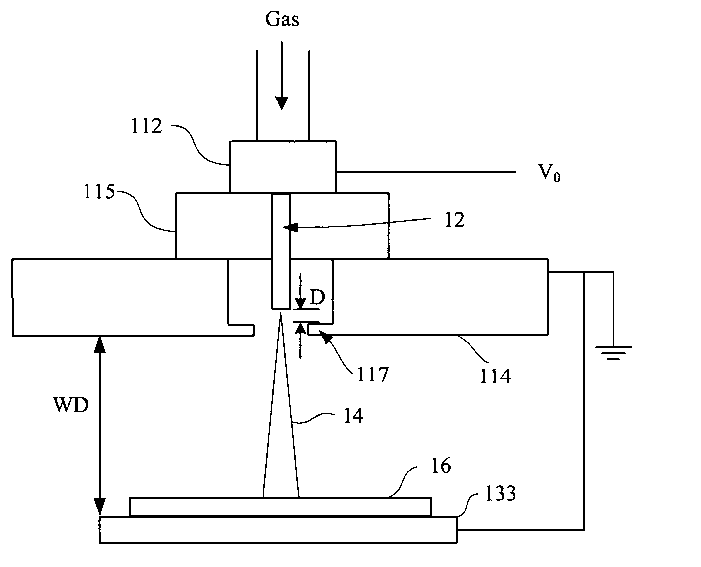
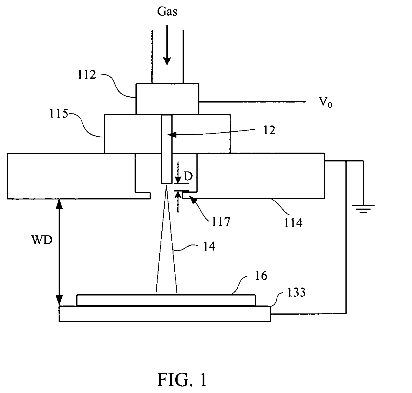
[0020]For manufacturing nanopins, the present invention utilizes crystal anisotropic hardness properties and increases the temperature of samples. For a zinc crystal lattice, the hardness of each crystal plane is somewhat different. Some crystal planes are fragile while zinc atoms on some crystal planes are bound strongly. When the zinc crystal lattice is bombarded by accelerated particles, for example, bombarded by an ion beam, zinc atoms on the fragile crystal planes are easy to be stuck out. But for the crystal planes with great hardness, the zinc crystal lattice is hard to be destructed when bombarded by the ion beam. Since the crystal lattice is at a scale of nanometers, the crystal anisotropic hardness properties can be utilized to fabricate nanopins. In addition, increasing temperature of a metal foil makes the diffusion of surface atoms increasing. Therefore, tip angles of nanopins, formed on the metal foil by ion source dry etching at high temperature, are smaller than thos...


PUM

PropertyMeasurementUnit
end radiusaaaaaaaaaa
aspect ratioaaaaaaaaaa

Abstract

Methods to manufacture metal nanopins and metal oxide nanopins are disclosed. Metal nanopins are fabricated on a metal foil by capillaritron plasma source dry etching. The aspect ratio and the density of metal nanopins are controlled by adjusting the temperature of the metal foil during ion beam dry etching. The end radius of metal nanopins less than 10 nm and the aspect ratio of metal nanopins between 25 and 30 can be achieved. Besides, metal oxide nanopins are fabricated by ion implantation and thermal oxidation. The metal foil is implanted with ions and then thermally oxidized to form the metal oxide nanopins. It shows that the metal oxide nanopins fabricated with oxygen implantation exhibit better field emission properties.

Description

TECHNICAL FIELD OF THE INVENTION[0001]The present invention relates to a nanopin manufacturing method, and more particularly, to a method that utilizes ion beam implantation and / or thermal oxidation for manufacturing nanopins. In addition, the present invention changes the temperature of sample for altering the nanopin tip angle.BACKGROUND OF THE INVENTION[0002]Flat panel displays have become mainstream products in the market. More and more types of flat panel displays are being marketed. For example, liquid crystal displays (LCDs) and emissive flat panel displays are two types of flat panel displays. Liquid crystal displays may be divided into groups such as thin-film transistor liquid crystal displays (TFT-LCDs), twisted nematic (TN) LCDs, super-twisted nematic (STN) LCDs, and ferroelectric liquid displays (FLCDs). A liquid crystal display needs a back-light source in rear of display panel for emitting light to display the contents shown in front of the panel. However, the transmi...

Claims


Application Information

Patent Timeline
Patent Type & Authority Patents(United States)
IPC IPC(8): B44C1/22
CPCB81C1/00111C23C14/086C23C14/48C23F4/00Y10S977/876
Inventor CHAO, LIANG-CHIUNLIAU, CHUNG-CHILEE, JUN-WEI
Owner NAT TAIWAN UNIV OF SCI & TECH
Why Eureka
Try Eureka