Double and triple gate MOSFET devices and methods for making same

a technology of mosfet and double gate metaloxide, which is applied in the direction of mosfet devices, semiconductor devices, electrical equipment, etc., can solve the problems of 0.1 m process generation and difficulty in scaling existing bulk mosfet devices beyond 0.1 m

Active Publication Date: 2012-07-17
ADVANCED MICRO DEVICES INC
View PDF24 Cites 20 Cited by
  • Summary
  • Abstract
  • Description
  • Claims
  • Application Information

AI Technical Summary

Benefits of technology

[0004]Implementations consistent with the principles of the invention provide double gate and triple gate FinFET devices. Unlike conventional designs, each of the gates in the FinFET can independently control the FinFET's channel.

Problems solved by technology

Due to limitations associated with gate-oxide thicknesses and source / drain (S / D) junction depths, scaling of existing bulk MOSFET devices beyond the 0.1 μm process generation may be difficult, if not impossible.

Method used


Image

  • Double and triple gate MOSFET devices and methods for making same
  • Double and triple gate MOSFET devices and methods for making same
  • Double and triple gate MOSFET devices and methods for making same

Examples


Embodiment Construction

[0016]The following detailed description of implementations consistent with the present invention refers to the accompanying drawings. The same reference numbers in different drawings may identify the same or similar elements. Also, the following detailed description does not limit the invention. Instead, the scope of the invention is defined by the appended claims and their equivalents.

[0017]Implementations consistent with the principles of the invention provide double gate and triple gate FinFET devices. Unlike conventional designs, each of the gates in the FinFET can independently control the fin channel.

EXEMPLARY PROCESSING

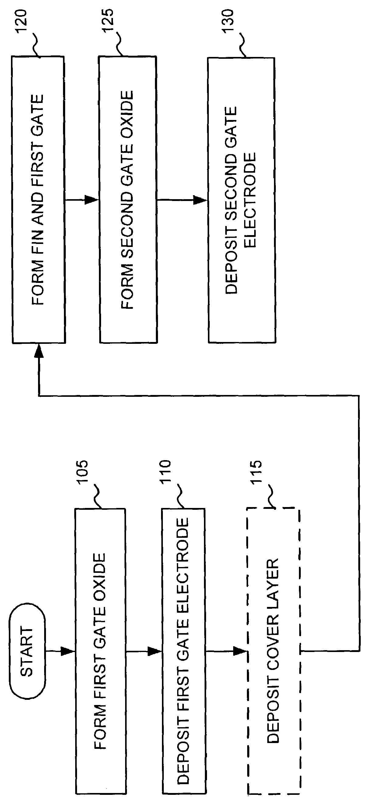
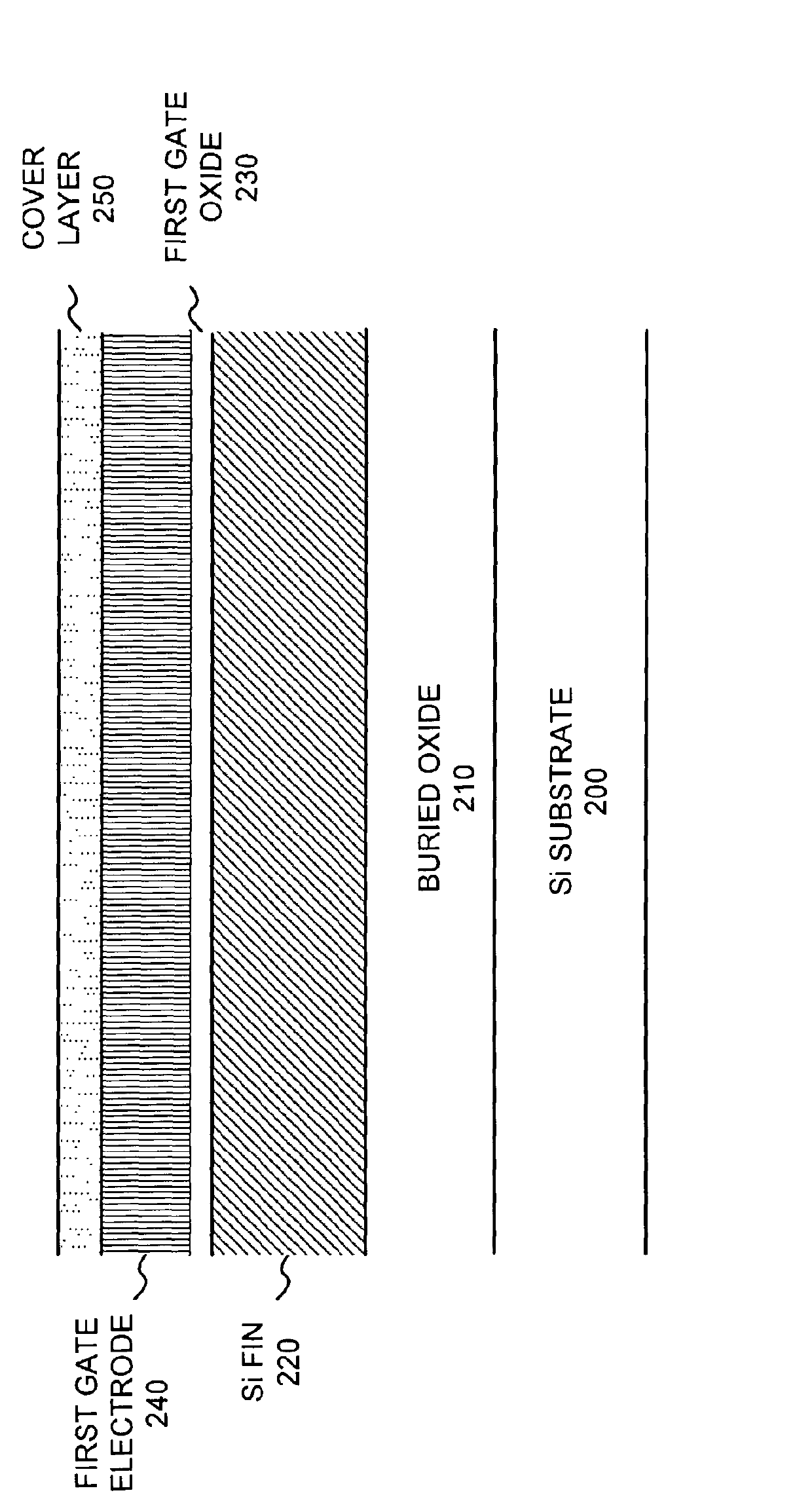
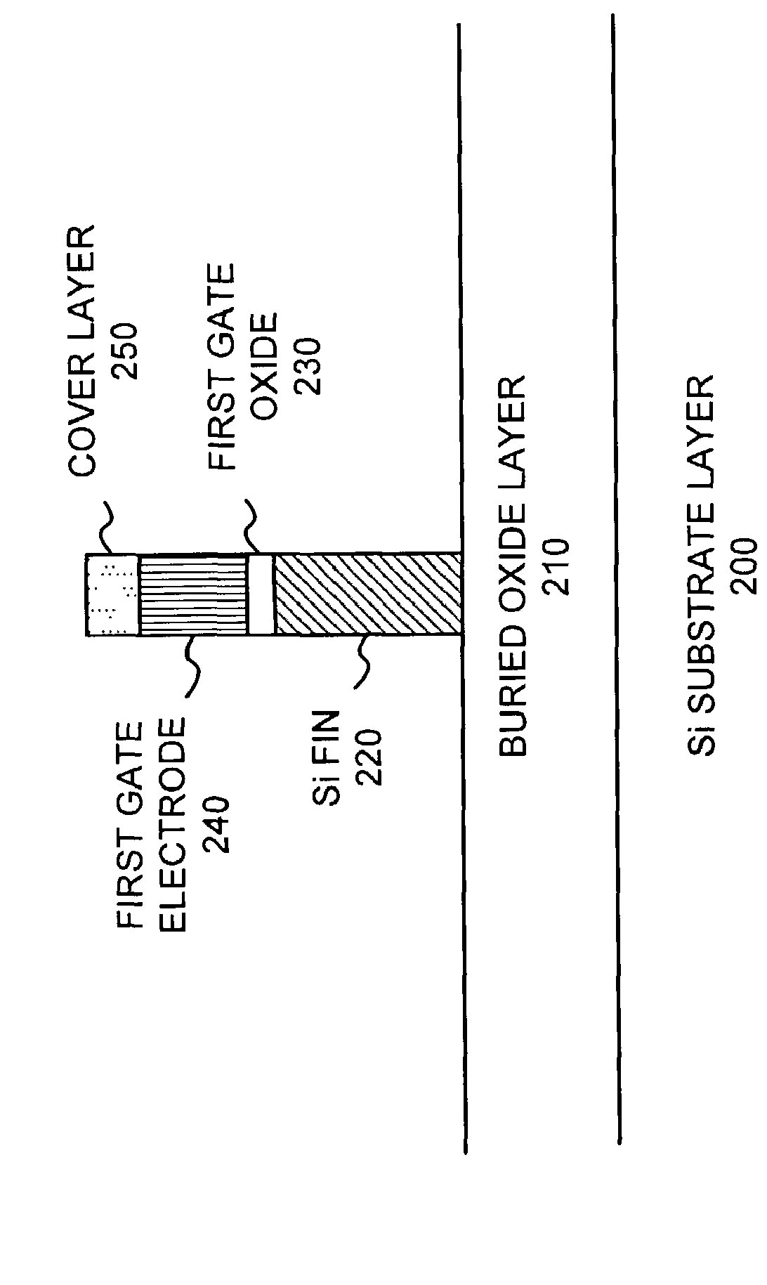
[0018]FIG. 1 illustrates an exemplary process for fabricating a double gate MOSFET in an implementation consistent with the principles of the invention. FIGS. 2-4 illustrate exemplary cross-sectional views of a MOSFET fabricated according to the processing described in FIG. 1.

[0019]With reference to FIGS. 1 and 2, processing may begin with a silicon on insulat...


PUM


Abstract

A double gate metal-oxide semiconductor field-effect transistor (MOSFET) includes a fin, a first gate and a second gate. The first gate is formed on top of the fin. The second gate surrounds the fin and the first gate. In another implementation, a triple gate MOSFET includes a fin, a first gate, a second gate, and a third gate. The first gate is formed on top of the fin. The second gate is formed adjacent the fin. The third gate is formed adjacent the fin and opposite the second gate.

Description

FIELD OF THE INVENTION[0001]The present invention relates generally to semiconductor manufacturing and, more particularly, to double and triple gate metal-oxide semiconductor field-effect transistor (MOSFET) devices and methods of making these devices.BACKGROUND OF THE INVENTION[0002]Scaling of device dimensions has been a primary factor driving improvements in integrated circuit performance and reduction in integrated circuit cost. Due to limitations associated with gate-oxide thicknesses and source / drain (S / D) junction depths, scaling of existing bulk MOSFET devices beyond the 0.1 μm process generation may be difficult, if not impossible. New device structures and new materials, thus, are likely to be needed to improve FET performance.[0003]Double-gate MOSFETs represent new devices that are candidates for succeeding existing planar MOSFETs. In double-gate MOSFETs, the use of two gates to control the channel significantly suppresses short-channel effects. A FinFET is a recent doubl...

Claims


Application Information

Patent Timeline
Patent Type & Authority Patents(United States)
IPC IPC(8): H01L29/72H01L21/336H01L29/423H01L29/786
CPCH01L29/42384H01L29/785H01L29/66818H01L29/66795H01L29/7855
Inventor LIN, MING-RENAN, JUDY XILINKRIVOKAPIC, ZORANTABERY, CYRUS E.WANG, HAIHONGYU, BIN
Owner ADVANCED MICRO DEVICES INC
Why Eureka
Try Eureka