Low lag transfer gate device

a transfer gate and low lag technology, applied in semiconductor devices, radio frequency controlled devices, electrical devices, etc., can solve problems such as image lag, pixel unusability, and leakage of bright point defects

Active Publication Date: 2012-07-24
GLOBALFOUNDRIES US INC
View PDF20 Cites 44 Cited by
  • Summary
  • Abstract
  • Description
  • Claims
  • Application Information

AI Technical Summary

Benefits of technology

[0018]The CMOS active pixel sensor (APS) cell structure has a transfer gate device comprising a gate dielectric layer formed on a substrate and a gate conductor layer formed on the gate dielectric layer, the gate conductor layer having a first doped region of first conductivity type material and a second doped region of a second conductivity type material. A photosensing device is formed at or below a substrate surface adjacent the first doped region of the transfer gate device for collecting charge carriers in response to light incident thereto, and, a diffusion region of a second conductivity type material is formed at or below the substrate surface adjacent the second doped region of the transfer gate device. The transfer gate device forms a channel region enabling charge transfer between the photosensing device and the diffusion region. After performing charge carrier collection at the photosensing device, a two-phase voltage bias is applied to the first and second transfer gate electrodes for forcing collected charge carriers from the photosensing device to the diffusion region while preventing spillback of charges to the photosensing device.
[0042]a light shield element for preventing incident light from reaching the second doped region of a second conductivity type material of the first gate conductor structure.

Problems solved by technology

Additionally, in the design of the CMOS APS cell 10′ it has been noticed that the presence of silicide contact regions (not shown) formed over the floating node diffusions, in the array, causes a bright point defect leakage problem.
That is, due to the additional presence of formed silicide contacts over these diffusions, it has been found that occasional pixels see silicide “spikes” which leak current at levels high enough to make that pixel unusable.
However, the pinned photodiode configuration may cause image lag due to the incomplete transfer of charge from the photodiode to the floating node.
That is, it is currently difficult to get low lag when pulling charge from a source / drain combination that is not essentially assymmetric.
This is because it is difficult to extract charges from a photodiode without some of the charges “spilling back” into the photodiode when the transfer gate is turned off.
However, with both the source / drain and the poly doping approaches, there is a trade off between “spillback” lag and photodiode reset-ability.
Spill back goes away, but it is hard to extract all the carriers out of the photodiode due to the high barrier.
Unfortunately, however, with the absence of the silicide from imagers with a transfer gate having n and p regions, each CMOS APS cell gate polysilicon formed with the built-in diode within the gate prevents the entire gate from being contacted.
That is, a contact which only connects either the n-type or p-type side of the polysilicon gate will not be adequately connected to the other polarity of the gate poly layer.
This results in a time dependent voltage on the uncontacted portion of the gate.
While a FET transistor device having a gate in the form of a diode is known in the art, there is currently no such teaching of a photocell structure having a diodic transfer gate having anode and cathode regions that are both contacted separately or biased differently and, switched and biased in a timed manner to address the “spillback” lag and photodiode reset-ability aspects of the image sensor device.

Method used


Image

  • Low lag transfer gate device
  • Low lag transfer gate device
  • Low lag transfer gate device

Examples


first embodiment

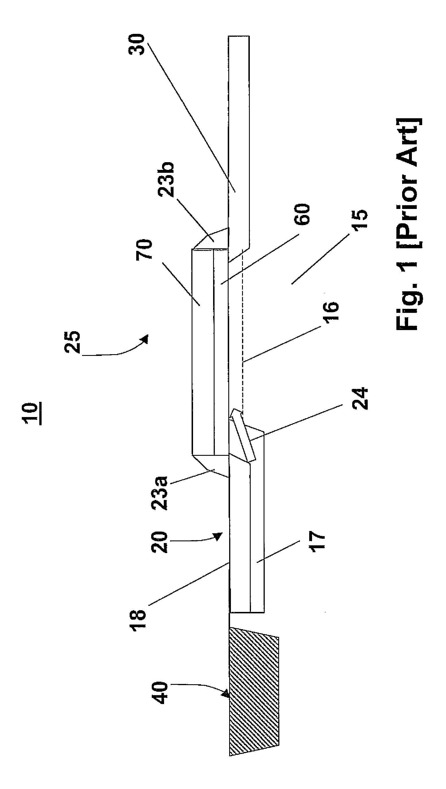
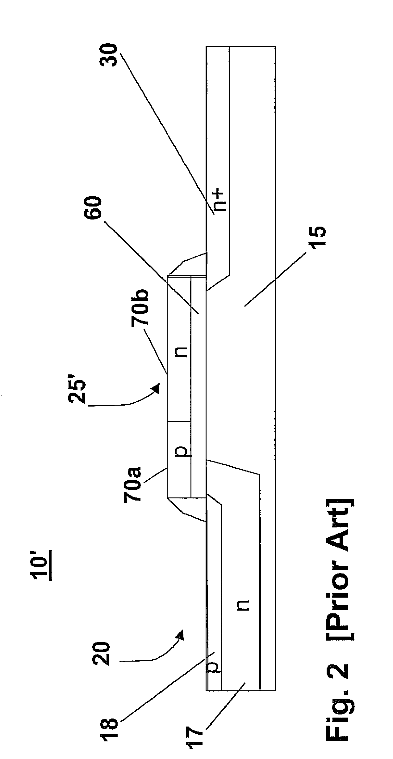
[0060]Co-pending U.S. patent application Ser. No. 11 / 565,801 entitled “SILICIDE STRAPPING IN IMAGER TRANSFER GATE DEVICE” describes a CMOS active pixel sensor (APS) cell structure having dual workfunction transfer gate device and method of fabrication. The transfer gate device comprises a dielectric layer formed on a substrate and a dual workfunction gate conductor layer formed on the dielectric layer comprising a first conductivity type doped region and an abutting second conductivity type doped region. The transfer gate device defines a channel region where charge accumulated by a photosensing device is transferred to a diffusion region. The disclosed APS cell structure includes a silicide structure formed atop the dual workfunction gate conductor layer for electrically coupling the first and second conductivity type doped regions for improved gate barrier ac characteristics. FIG. 3 illustrates, through a cross-sectional view, a CMOS imager APS 100 including photosensing device, e...

second embodiment

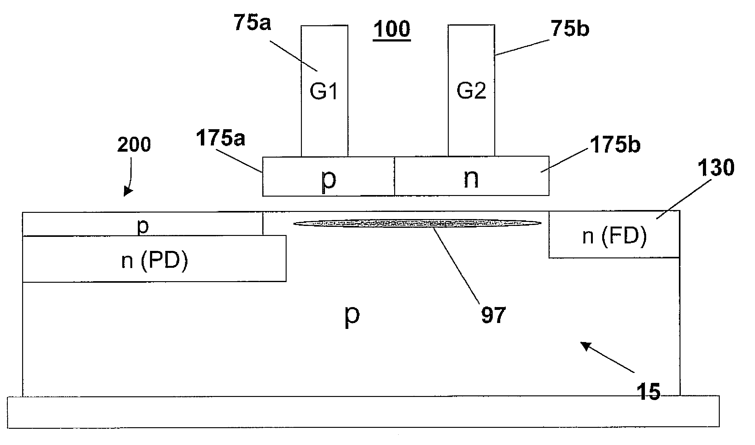
[0061]In an alternate embodiment of the invention, instead of a diodic transfer gate structure, the transfer gate comprises two distinct gate structures separated by a small distance with each gate structure doped with opposite conductivity type. More specifically, FIG. 4 illustrates, through a cross-sectional view, a back end of line CMOS imager APS 100′ including photosensing device, e.g., photodiode 200 formed at one side of a silicon-containing, e.g., polysilicon, transfer gate device 125′ according to the invention, and, an n-type floating diffusion region130 at the other side of the transfer gate 125′. The polysilicon transfer gate 125′ includes a first p-type doped gate structure 176a and a second n-type doped gate structure 176b separated a small distance which, in one embodiment, may be 200 nm or less, e.g., about 100 nm, although, it is understood that there is no minimum spacing, just minimum resolvable image sizes. Each of the doped gate structures are formed over the th...


PUM


Abstract

A CMOS active pixel sensor (APS) cell structure includes at least one transfer gate device and method of operation. A first transfer gate device comprises a diodic or split transfer gate conductor structure having a first doped region of first conductivity type material and a second doped region of a second conductivity type material. A photosensing device is formed adjacent the first doped region for collecting charge carriers in response to light incident thereto, and, a diffusion region of a second conductivity type material is formed at or below the substrate surface adjacent the second doped region of the transfer gate device for receiving charges transferred from the photosensing device while preventing spillback of charges to the photosensing device upon timed voltage bias to the diodic or split transfer gate conductor structure.

Description

CROSS-REFERENCE TO RELATED APPLICATION[0001]The present invention claims the benefit of commonly-owned, co-pending U.S. patent application Ser. No. 12 / 013,826 entitled “A LOW LAG TRANSFER GATE DEVICE” filed concurrently with this application, the whole contents and disclosure of which is expressly incorporated by reference herein as if fully set forth herein.FIELD OF THE INVENTION[0002]The present invention relates to semiconductor optical image sensors, and particularly, to a novel CMOS (complementary metal oxide semiconductor) image sensor cell structure including a transfer gate device exhibiting reduced lag, higher capacity and lower dark current.DESCRIPTION OF THE PRIOR ART[0003]CMOS image sensors are now replacing conventional CCD sensors for applications requiring image pick-up such as digital cameras, mobile telephones, cellular telephones, pervasive digital devices such as PDA's (personal digital assistant), personal computers, medical devices, and the like. Advantageously,...

Claims


Application Information

Patent Timeline
Patent Type & Authority Patents(United States)
IPC IPC(8): H01L31/062H01L31/113H01L27/148H01L21/00
CPCH01L27/14603H01L27/14612H01L27/14609
Inventor ADKISSON, JAMES W.BRYANT, ANDRESELLIS-MONAGHAN, JOHN J.
Owner GLOBALFOUNDRIES US INC
Why Eureka
Try Eureka