Foundry compatible process for manufacturing a magneto meter using lorentz force for integrated systems

Active Publication Date: 2012-08-07
MOVELLA INC
View PDF9 Cites 44 Cited by
  • Summary
  • Abstract
  • Description
  • Claims
  • Application Information

AI Technical Summary

Benefits of technology

[0009]Many benefits are achieved by way of the present invention over conventional techniques. For example, the present technique provides an easy to use process that relies upon conventional technology. In some embodiments, the method provides higher device yields in dies per wafer with the integrated approach. Additionally, the method provides a process and system that are compatible with conventional pro

Problems solved by technology

Although highly successful, ICs and in particular MEMS still have limitations.
Similar to IC development, MEMS development, which focuses on increasing performance, reducing size, and decreasing cost, con

Method used


Image

  • Foundry compatible process for manufacturing a magneto meter using lorentz force for integrated systems
  • Foundry compatible process for manufacturing a magneto meter using lorentz force for integrated systems
  • Foundry compatible process for manufacturing a magneto meter using lorentz force for integrated systems

Examples


Embodiment Construction

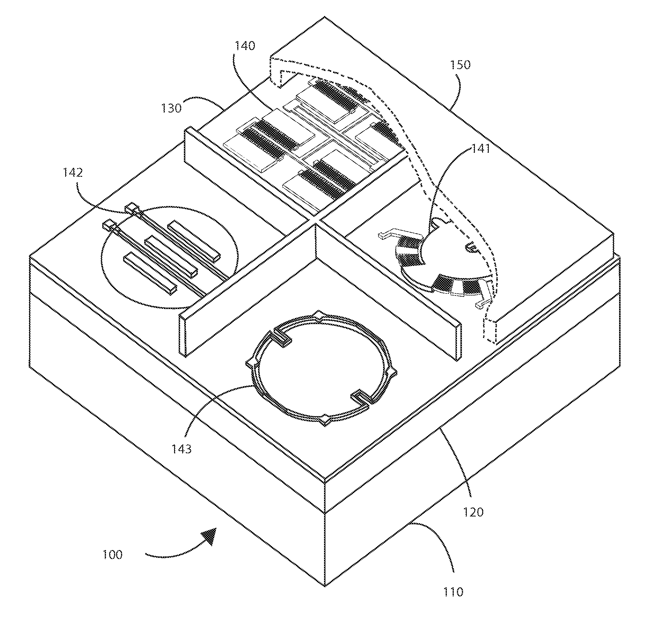
[0035]According to the present invention, techniques related generally to electronic and mechanical devices are provided. More particularly, the present invention provides a method of fabricating an electronic compass that is preferably integrated with one or more integrated circuits and other micro-electrical mechanical systems, commonly termed MEMS. Merely by way of example, the MEMS devices can include at least an accelerometer, a gyroscope, a magnetic sensor, a pressure sensor, a microphone, a humidity sensor, a temperature sensor, a chemical sensor, a biosensor, an inertial sensor, and others. Additionally, the other applications include at least a sensor application or applications, system applications, and broadband applications, among others. But it will be recognized that the invention has a much broader range of applicability.

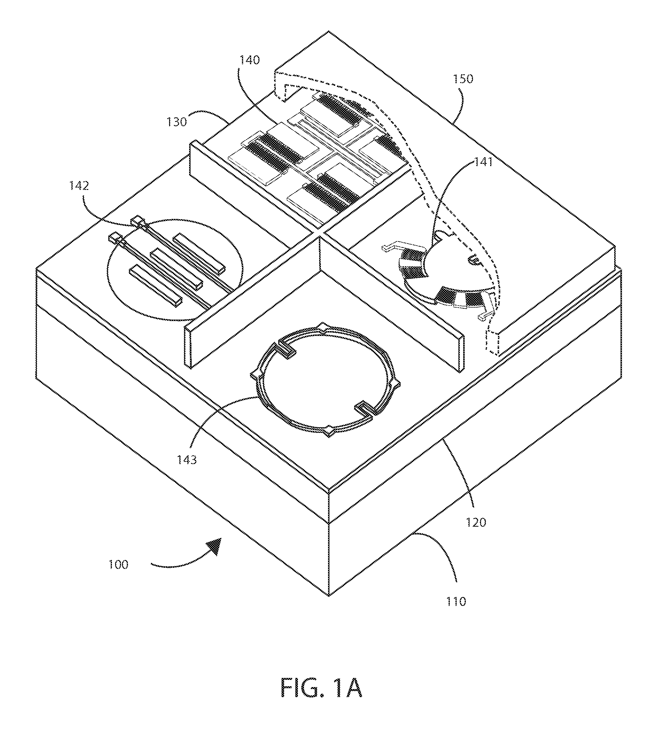
[0036]FIG. 1A is a simplified perspective diagram of an integrated MEMS and circuit system according to an embodiment of the present invention. This ...


PUM


Abstract

A method for fabricating an integrated electronic compass and circuit system. The fabrication method begins with providing a semiconductor substrate comprising a surface region. One or more CMOS integrated circuits are then formed on one or more portions of the semiconductor substrate. Once the CMOS circuits are formed, a thickness of dielectric material is formed overlying the one or more CMOS integrated circuits. A substrate is then joined overlying the thickness of the dielectric material. Once joined, the substrate is thinned to a predetermined thickness. Following the thinning process, an electric compass device is formed within one or more regions of the predetermined thickness of the substrate. Other mechanical devices or MEMS devices can also be formed within one or more regions of the thinned substrate.

Description

CROSS-REFERENCES TO RELATED APPLICATIONS[0001]The present application claims priority to and incorporates by reference, for all purposes, the following pending patent application: U.S. Pat. App. No. 61 / 295,673, filed Jan. 15, 2010. The present invention also incorporates by reference, for all purposes, the following patent applications: U.S. patent application Ser. No. 12 / 859,631, filed Aug. 19, 2010, U.S. Pat. application Ser. No. 12 / 490,067, filed Jun. 23, 2009, U.S. patent application Ser. No. 12 / 957,222, filed Nov. 30, 2010, U.S. Pat. App. No. 61 / 367,032, filed Jul. 23, 2010, U.S. patent application Ser. No. 12 / 945,087, filed Nov. 12, 2010, and U.S. patent application Ser. No. 12 / 913,440, filed Oct. 27, 2010.BACKGROUND OF THE INVENTION[0002]Embodiments of the present invention relates generally to electronic and mechanical devices technologies. More particularly, embodiments of the present invention provide a method for fabricating an electronic compass device that is preferably...

Claims


Application Information

Patent Timeline
IPC IPC(8): H01L21/00
CPCB81C1/00238G01R33/0283G01C25/00G01C17/28
Inventor HSU, GEORGEYANG, XIAO "CHARLES"
Owner MOVELLA INC
Why Eureka
Try Eureka