
Image encoding device, image processing device, image display device, image encoding method, and image processing method

a technology of image data and encoding method, which is applied in the direction of electric digital data processing, instruments, computing, etc., can solve the problems of increasing the cost of a liquid crystal display device, unable to display a fast-varying motion picture of high quality, etc., and achieves the effect of suppressing an encoding error, reducing an amount of encoded image data, and reducing an encoding error

Inactive Publication Date: 2012-08-07
MITSUBISHI ELECTRIC CORP
View PDF34 Cites 4 Cited by
  • Summary
  • Abstract
  • Description
  • Claims
  • Application Information

AI Technical Summary

Benefits of technology

This approach effectively reduces the amount of encoded image data while minimizing encoding errors, preventing unwanted overvoltage and maintaining display quality by dynamically adjusting pixel numbers based on block dynamic ranges.

Problems solved by technology

However, since a liquid crystal requires a given time after a drive voltage is applied to the liquid crystal until transmissivity of the liquid crystal reaches a predetermined level, the liquid crystal has a defect that it cannot display a fast-varying motion picture of high quality.
Such increased capacity of the frame memory and such increased data transmission rate lead to an increase in the cost of a liquid crystal display device.

Method used


Image

  • Image encoding device, image processing device, image display device, image encoding method, and image processing method
  • Image encoding device, image processing device, image display device, image encoding method, and image processing method
  • Image encoding device, image processing device, image display device, image encoding method, and image processing method

Examples


first embodiment

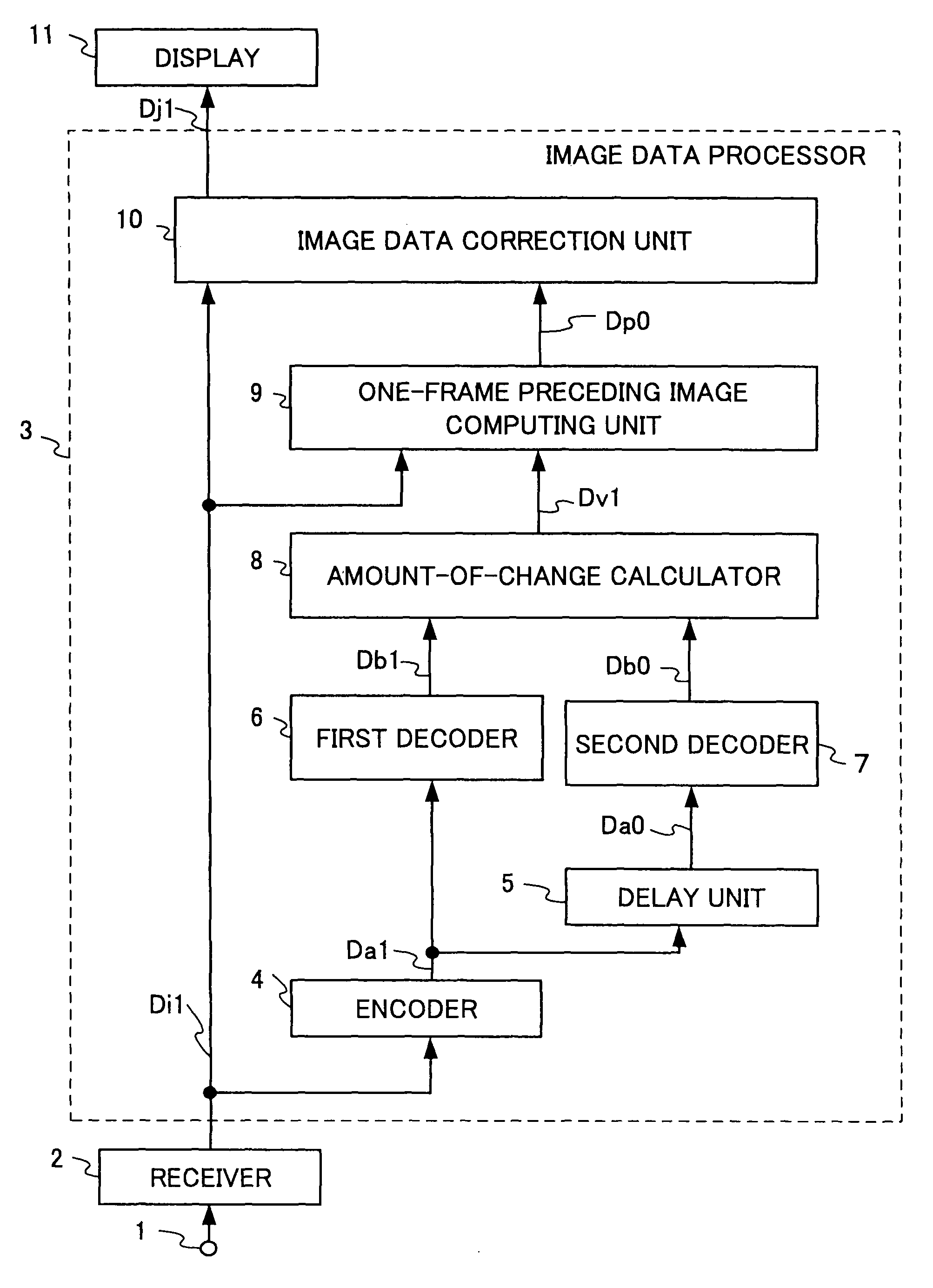
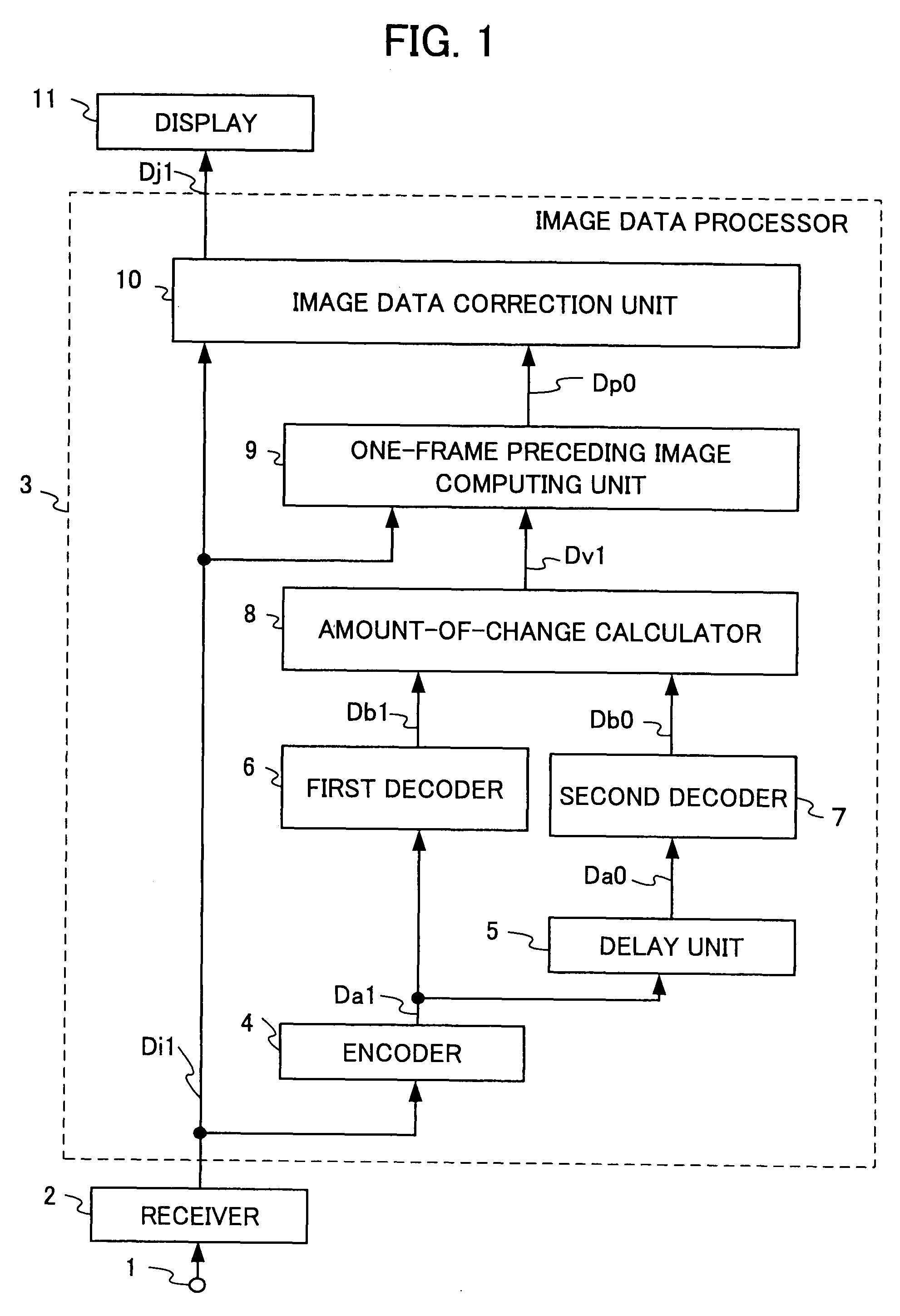
[0043]FIG. 1 is a block diagram showing a configuration of an image display device including an image data processor 3 which is an image processing device according to the first embodiment of the present invention. As shown in FIG. 1, the image display device includes, as its main constituent elements, a receiver 2, an image data processor 3, and a display 11. In this application, constituent elements shown by “ . . . unit”, “ . . . er” or “ . . . or” may be implemented in the form of hardware including an electric circuit or the like, in the form of software, or in the form of a combination of software and hardware. Further, the image data processor 3 is a device capable of implementing an image processing method of the present invention. Furthermore, the image display device shown in FIG. 1 is, for example, a liquid crystal television set.

[0044]The receiver 2 includes a television tuner and other elements. The receiver 2 receives a video signal through an input terminal 1, process...

second embodiment

[0084]FIG. 15 is a block diagram showing a configuration of an image display device including an image data processor 40 which is an image processing device according to the second embodiment of the present invention. In FIG. 15, constituent elements having the same as or corresponding to those in FIG. 1 are assigned the same reference numerals. The image data processor 40 of the second embodiment is different from the image data processor 3 of the aforementioned first embodiment in that the image data processor 40 includes a color space converter 41 at the preceding stage of the encoder 4, a color space converter 42 at the subsequent stage of the first decoder 6, and a color space converter 43 at the subsequent stage of the second decoder 7.

[0085]The color space converter 41 converts the current image data Di1 to image data of a brightness signal Y and color signals Cb and Cr, and outputs a converted current image data Dt1. The encoder 4 encodes the current image data Dt1 and outpu...

third embodiment

[0107]FIG. 18 is a block diagram showing a configuration of a liquid crystal display device including an image data processor 44 which is an image processing device according to the third embodiment of the present invention. In FIG. 18, constituent elements having the same as or corresponding to those in FIG. 1 are assigned the same reference numerals. The image data processor 44 of the image data processor 3 is different from the image data processor 3 of the first embodiment shown in FIG. 1, in that a first high frequency component emphasizer 45 is provided at the subsequent stage of the first decoder 6, a second high frequency component emphasizer 46 is provided at the subsequent stage of the second decoder 7, the decoded image data Db1 and the encoding parameter pb1 are inputted to the first high frequency component emphasizer 45 from the first decoder 6, the decoded image data Db0 and the encoding parameter Pb0 are outputted from the second decoder 7 to the second high frequenc...


PUM


Abstract

An image encoding device includes a dynamic range generator for outputting dynamic range data Dd1 of block image data Dc1, an average value generator for outputting average value data De1 of the block image data Dc1, a number-of-pixel reducing unit 20 for decreasing number of pixels of the block image data by reduction-number of pixels to generate reduced-number-of-pixel block image data Dc1′, an encoding parameter generator 18 for generating encoding parameter pa1 specifying a quantization bit rate and the reduction-number of pixels in accordance with the dynamic range data Dd1, a quantization threshold generator 19 for generating a quantization threshold value tb1, and an image data quantizer 21 for generating quantized image data Df1 from the reduced-number-of-pixel block image data Dc1′ with use of the quantization threshold value tb1.

Description

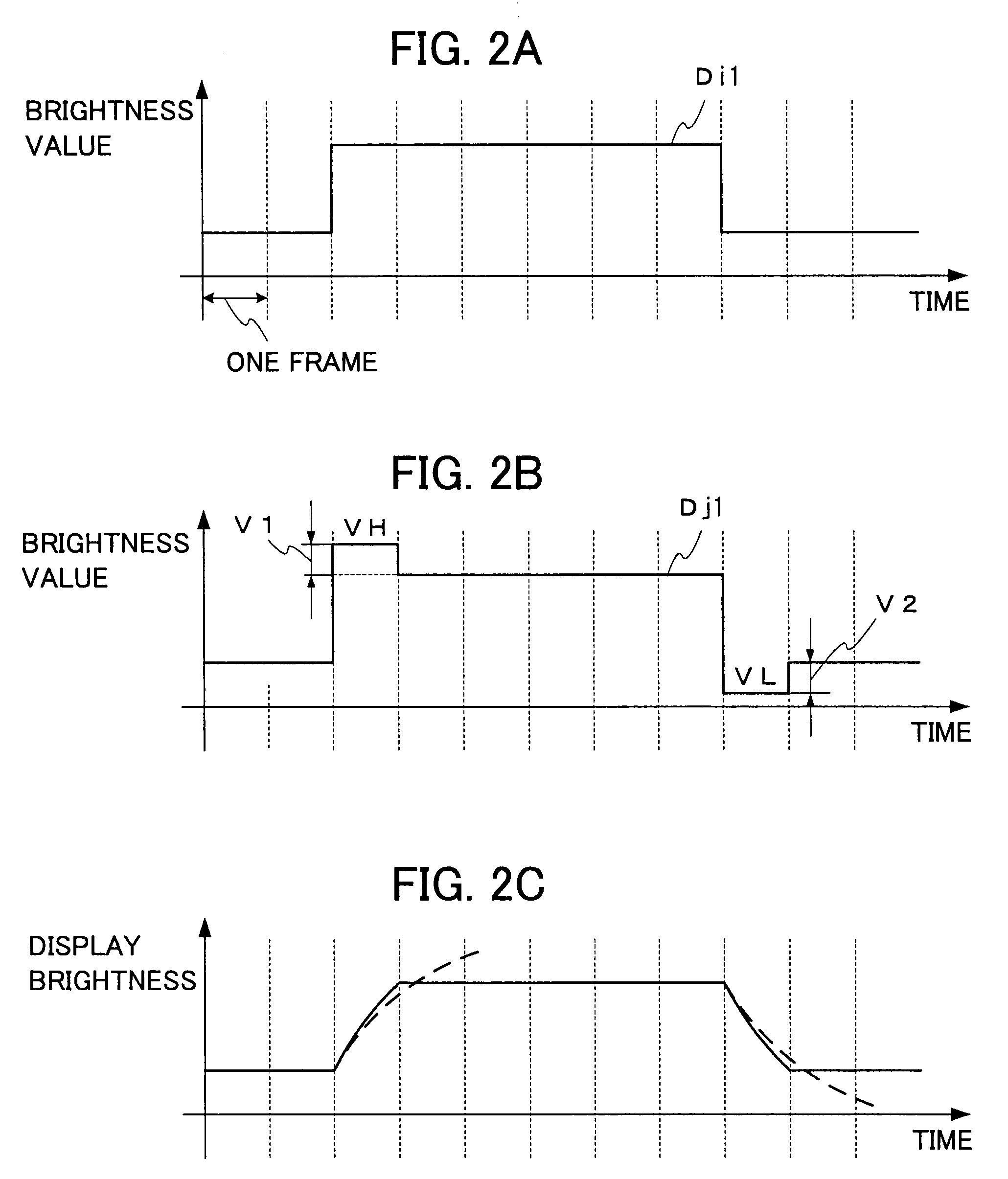
TECHNICAL FIELD[0001]The present invention relates to an image encoding device, an image processing device including the image encoding device, an image display device including the image processing device, an image encoding method, and an image processing method, which are used for encoding input image data on a block-by-block basis.BACKGROUND ART[0002]Since a liquid crystal panel is thin in thickness and light in weight, it is widely used as a display device such as a television receiver set, a computer display, a display of a personal digital assistant or the like. However, since a liquid crystal requires a given time after a drive voltage is applied to the liquid crystal until transmissivity of the liquid crystal reaches a predetermined level, the liquid crystal has a defect that it cannot display a fast-varying motion picture of high quality. In order to solve such a problem, when a gradation value varies between successive frames, a driving method, in which an overvoltage is a...

Claims


Application Information

Patent Timeline
Patent Type & Authority Patents(United States)
IPC IPC(8): G06F3/038H04N19/625H04N1/41H04N19/00H04N19/63H04N19/90H04N19/98
CPCH04N19/147H04N19/59H04N19/91H04N19/132H04N19/186H04N19/182H04N19/184H04N19/98H04N19/124G09G3/3611G09G2320/0252G09G2340/02G09G2340/16H04N19/61H04N19/176
Inventor NAGASE, AKIHIROSOMEYA, JUNOKUDA, NORITAKA
Owner MITSUBISHI ELECTRIC CORP
Learn More