Method for correcting mask pattern and method for manufacturing acceleration sensor and angular velocity sensor by using the method for correcting the mask pattern

a mask pattern and mask pattern technology, applied in the direction of acceleration measurement using interia forces, turn-sensitive devices, instruments, etc., can solve the problems of deteriorating etching accuracy, unwanted tapered and/or tilted portions, in-plane distribution of plasma changes, etc., to achieve accurate position control, small size, and high accuracy

Inactive Publication Date: 2012-08-14
DAI NIPPON PRINTING CO LTD
View PDF9 Cites 11 Cited by
  • Summary
  • Abstract
  • Description
  • Claims
  • Application Information

AI Technical Summary

Benefits of technology

[0014]The present invention was made in light of the above circumstances, and therefore it is an object of this invention to provide a new method for correcting the mask pattern used for dry-etching an object, such as the silicon wafer or the like, with higher accuracy. Another object of this invention is to provide a new method for readily manufacturing the acceleration sensor and / or angular velocity sensor, each having a significantly small size and excellent reliability.
[0020]As described above, the method according to the present invention is intended to control the formation of the tapered portion and tilted portion, not by controlling the apparatus and / or conditions employed or selected for the dry-etching process, but by correcting the opening of the mask pattern used for the dry-etching process, based on the distribution of the tapered portion and tilted portion, respectively detected in the surface of the wafer and peculiar to such apparatus and conditions. With this method, the dry-etching process can be provided to the silicon wafer with higher accuracy, thus achieving significantly accurate position control for the length of each beam as well as for the center of gravity of the weight. Additionally or alternatively, this invention is intended for providing the method for manufacturing the acceleration sensor and / or angular velocity sensor having a significantly small size and higher reliability.

Problems solved by technology

However, in a usual dry-etching process provided to the silicon wafer, the plasma may tend to be non-uniform in the surface of the silicon wafer, resulting in some in-plane distribution of the plasma changing from the center of the silicon wafer toward the periphery thereof.
Thus, an unwanted tapered and / or tilted portion is formed in each necessary hole or opening formed by the etching.
This leads to deterioration of accuracy of the etching.
Accordingly, such a tapered portion should make it difficult to form each weight as designed in advance.
Such a tilted portion should shift the center of gravity of each weight from a designed position (desired position) thereof, leading to deterioration of operational properties of the sensor.
However, it is quite difficult to successfully prevent the formation of the tapered and tilted portions, by only controlling the apparatus and / or process conditions.

Method used


Image

  • Method for correcting mask pattern and method for manufacturing acceleration sensor and angular velocity sensor by using the method for correcting the mask pattern
  • Method for correcting mask pattern and method for manufacturing acceleration sensor and angular velocity sensor by using the method for correcting the mask pattern
  • Method for correcting mask pattern and method for manufacturing acceleration sensor and angular velocity sensor by using the method for correcting the mask pattern

Examples


Embodiment Construction

[0039]Hereinafter, one exemplary embodiment of the present invention will be described, with reference to the drawings.

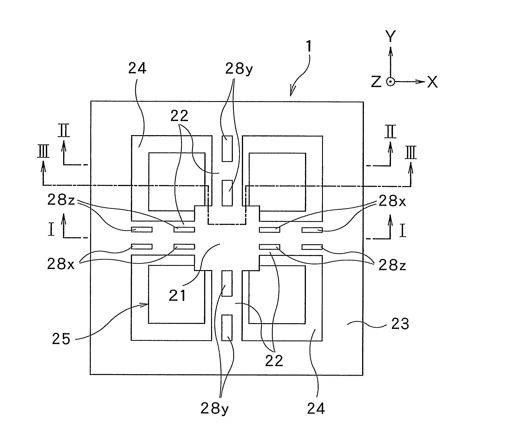
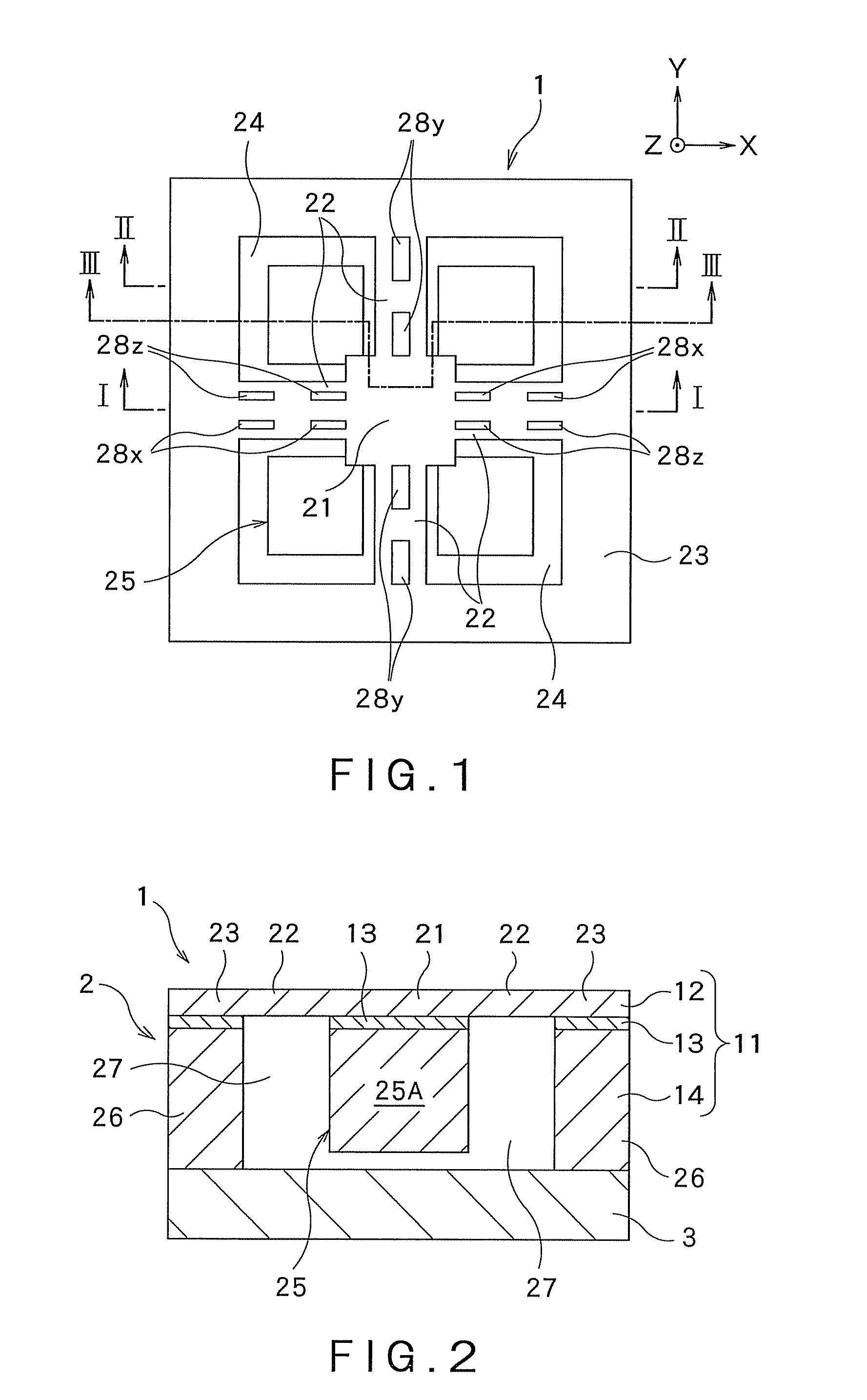
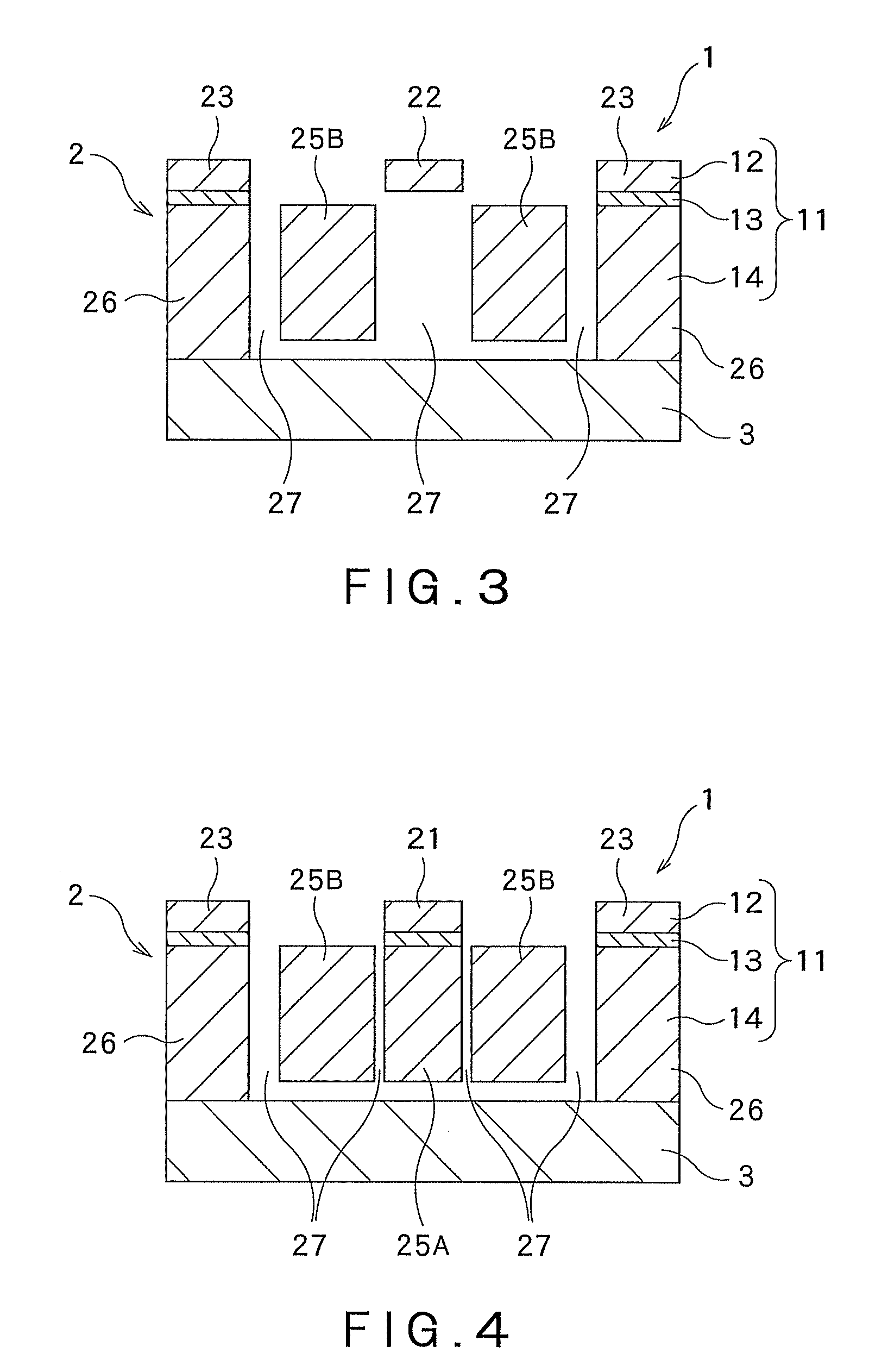
[0040]FIG. 1 is a plan view of a piezo-resistance-type acceleration sensor, which is one example of sensors manufactured by a method according to the present invention, FIG. 2 is a cross section, taken along line I-I, of the sensor shown in FIG. 1, FIG. 3 is a cross sectional view, taken along line II-II, of the sensor shown in FIG. 1, and FIG. 4 is a cross sectional view, taken along line III-III, of the sensor shown in FIG. 1. In these drawings, the sensor 1 includes a sensor body 2 and a supporting substrate 3 joined to the sensor body 2. The sensor body 2 is formed of an SOI (Silicon On Insulator) substrate 11 having a three-layer structure including a silicon-oxide layer 13 interposed between a silicon layer 12 (or active-layer silicon) and another silicon layer 14 (or base silicon). FIG. 5 is a perspective view of the sensor 1 shown in FIG. 1, and FIG. 6 is an...


PUM

PropertyMeasurementUnit
thicknessaaaaaaaaaa
diameteraaaaaaaaaa
weightaaaaaaaaaa

Abstract

A method for correcting a mask pattern used for dry-etching an object with higher accuracy, and for manufacturing an acceleration sensor and an angular velocity sensor. The object is first etched by a dry-etching process using an uncorrected reference mask pattern. Then, distribution of the size of expansion of a tapered portion formed in a surface of the object is measured. Thereafter, the measured distribution is approximated by using a quadratic curve (Y=AX2+B) so as to determine A and B. Consequently, an amount t of correction for the tapered portion, which is expressed by the following equation (1) and related to a width of an opening of the mask pattern in a position at a distance r from a center of the object to be etched, can be set. In this way, the correction for the tapered portion can be carried out.t=(Ar2+B) / 2  (1)

Description

BACKGROUND OF THE INVENTION[0001]1. Field of the Invention[0002]The present invention relates to a method for correcting a mask pattern used for dry-etching a silicon wafer or the like, and also relates to a method for manufacturing an acceleration sensor and / or angular velocity sensor by using the method for correcting the mask pattern.[0003]2. Background Art[0004]In recent years, development of a small-sized sensor utilizing the so-called MEMS (Micro Electromechanical Systems) technology has been advanced, wherein application of a sensor for detecting acceleration and / or angular velocity to various devices or machines, such as portable phones and / or game machines, has been studied. Generally, the acceleration sensor and / or angular velocity sensor of this type is manufactured by using an SOI wafer having a three-layer structure composed of a silicon layer, a silicon-oxide layer and another silicon layer. More specifically, the sensor of this type includes a frame having an opening ...

Claims


Application Information

Patent Timeline
Patent Type & Authority Patents(United States)
IPC IPC(8): H01L21/00G01C19/56G01P15/12G01P15/125G01P15/18G03F1/00G03F1/68H01L21/3065H01L29/84
CPCG01C19/5719G01C25/00G01P15/0802G01P15/123G01P15/125G01P2015/0828G01P2015/0842
Inventor MORII, AKIO
Owner DAI NIPPON PRINTING CO LTD
Why Eureka
Try Eureka