Supercharge Your Innovation With Domain-Expert AI Agents!

Write-pattern determination for maskless lithography

a write-pattern and maskless technology, applied in the field of write-pattern determination of maskless lithography, can solve the problems of time-consuming and expensive design and manufacture of photo-masks, accompanied by unwanted distortions and artifacts, and difficult to design and manufacture photo-masks

Inactive Publication Date: 2012-08-14
DINO TECH ACQUISITION
View PDF28 Cites 4 Cited by
  • Summary
  • Abstract
  • Description
  • Claims
  • Application Information

AI Technical Summary

Benefits of technology

This approach enables accurate and efficient generation of write patterns that improve resolution and process window in maskless lithography, reducing the need for photo-masks and addressing distortions, while allowing dynamic adjustment of spatial-light modulators during the lithography process.

Problems solved by technology

Unfortunately, it is increasingly difficult to design and manufacture photo-masks.
However, due to the wave nature of light, as dimensions approach sizes comparable to the wavelength of the light used in the photolithography process, the resulting wafer patterns deviate from the corresponding photo-mask patterns and are accompanied by unwanted distortions and artifacts.
Furthermore, the design and manufacture of photo-masks is time consuming and expensive.
This poses a significant challenge during integrated-circuit development and for the production of small quantities of integrated-circuit dies or the semiconductor wafers.
Unfortunately, existing techniques first determine mask patterns, which are then converted into write patterns.
This is cumbersome and often ignores characteristics of the spatial-light modulators when the mask patterns are determined.
Furthermore, the bifurcated-design technique may make it more difficult to improve resolution and / or a process window in a lithography process by appropriately pre-distorting the write pattern (using techniques such as Optical Proximity Correction or OPC) such that the wafer pattern is printed more accurately.

Method used


Image

  • Write-pattern determination for maskless lithography
  • Write-pattern determination for maskless lithography
  • Write-pattern determination for maskless lithography

Examples


Embodiment Construction

[0056]The following description is presented to enable any person skilled in the art to make and use the invention, and is provided in the context of a particular application and its requirements. Various modifications to the disclosed embodiments will be readily apparent to those skilled in the art, and the general principles defined herein may be applied to other embodiments and applications without departing from the spirit and scope of the present invention. Thus, the present invention is not intended to be limited to the embodiments shown, but is to be accorded the widest scope consistent with the principles and features disclosed herein.

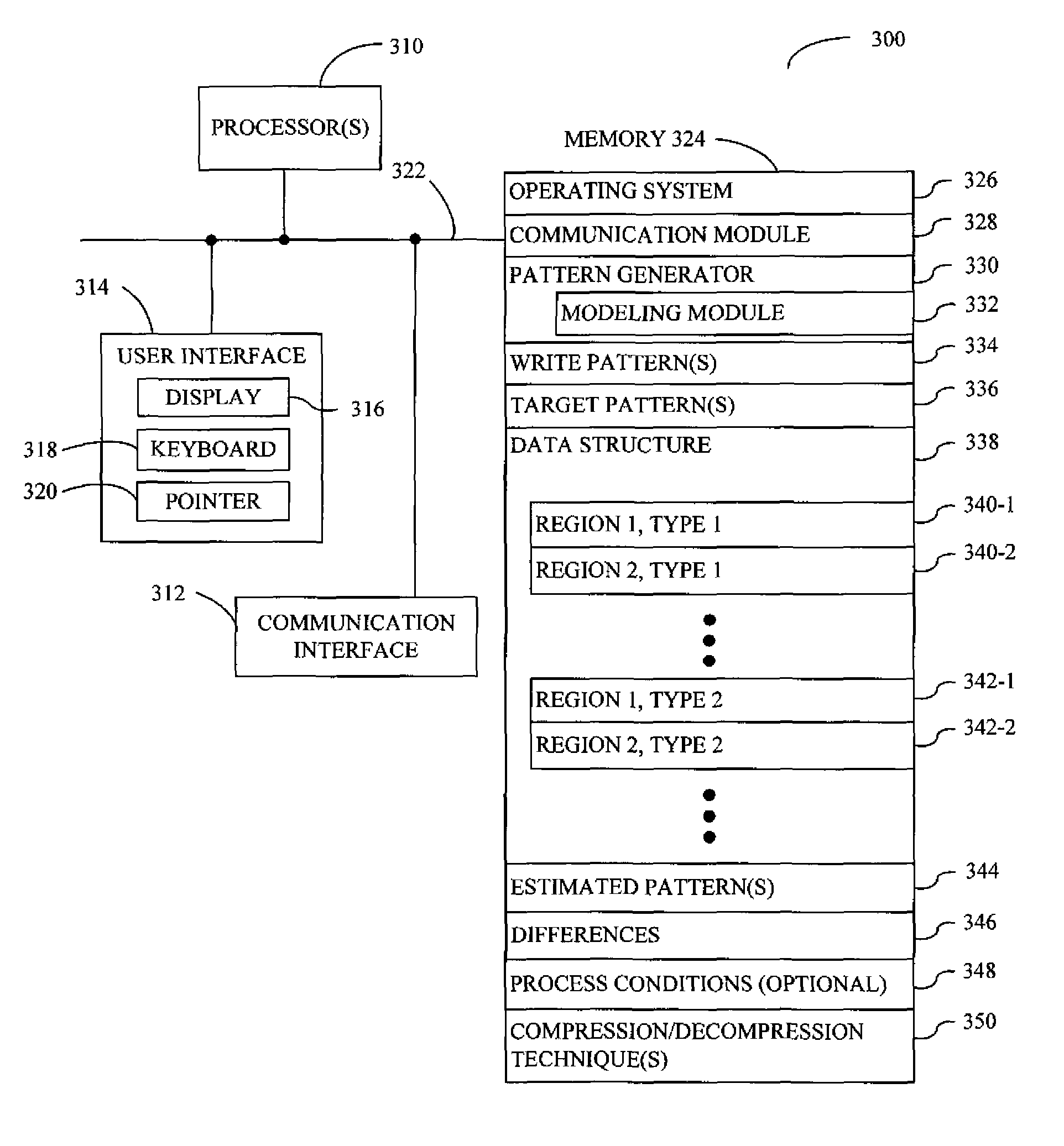
[0057]Embodiments of a write device, a computer system, a method, and a computer program product (i.e., software), and data structures or files for use with the write device and / or computer system are described. These systems, processes, and data structures may be used to determine write patterns that, in turn, may be used when producing integr...


PUM


Abstract

A method for generating a write pattern to be used in a maskless-lithography process is described. During the method, a computer system determines a one-to-one correspondence between pixels in the write pattern and at least a subset of elements in a spatial-light modulator used in the maskless-lithography process. Furthermore, the computer system generates the write pattern. Note that the write pattern includes features corresponding to at least the subset of elements in the spatial-light modulator, and the generating is in accordance with a characteristic dimension of an element in the spatial-light modulator and a target pattern that is to be printed on a semiconductor wafer during the maskless-lithography process.

Description

CROSS-REFERENCE[0001]This application claims the benefit of U.S. Provisional Application No. 60 / 972,676, filed Sep. 14, 2007, which application is incorporated herein by reference.FIELD OF THE INVENTION[0002]This application is related to copending patent application Ser. No. 12 / 206,660 for Write-Pattern Determination for Maskless Lithography, invented by Daniel S. Abrams and Timothy Lin.BACKGROUND[0003]1. Field of the Invention[0004]The present invention relates to techniques for determining write patterns for maskless-lithography processes that use write devices.[0005]2. Related Art[0006]Lithography processing represents an essential technology for manufacturing Integrated Circuits (IC) and Micro Electro-Mechanical Systems (MEMS). Lithographic techniques are used to define patterns, geometries, features, shapes, etc. (henceforth referred to as ‘patterns’) onto an integrated-circuit die, semiconductor wafer, or chips, where the patterns are typically defined by a set of contours, l...

Claims


Application Information

Patent Timeline
Patent Type & Authority Patents(United States)
IPC IPC(8): G06F17/50
CPCG03F7/70116G03F7/70291G03F7/70508
Inventor ABRAMS, DANIEL S.LIN, TIMOTHY
Owner DINO TECH ACQUISITION
Features
  • R&D
  • Intellectual Property
  • Life Sciences
  • Materials
  • Tech Scout
  • Unparalleled Data Quality
  • Higher Quality Content
  • 60% Fewer Hallucinations
Learn More