Method for making field emission device

a field emission device and emission method technology, applied in the manufacture of electrode systems, electric discharge tubes/lamps, discharge tubes luminescnet screens, etc., can solve the problem of short lifespan of field emission devices

Active Publication Date: 2012-08-21
TSINGHUA UNIV +1
View PDF8 Cites 1 Cited by
  • Summary
  • Abstract
  • Description
  • Claims
  • Application Information

AI Technical Summary

Problems solved by technology

The carbon nanotubes become damaged, thus causing the field emission device to have a short lifespan.

Method used


Image

  • Method for making field emission device
  • Method for making field emission device
  • Method for making field emission device

Examples


Embodiment Construction

[0020]The disclosure is illustrated by way of example and not by way of limitation in the figures of the accompanying drawings in which like references indicate similar elements. It should be noted that references to “an” or “one” embodiment in this disclosure are not necessarily to the same embodiment, and such references mean at least one.

[0021]References will now be made to the drawings to describe, in detail, various embodiments of the present field emission device, method for making the same, and ion source using the same. The field emission device can include a single unit or a number of units to form an array. In following embodiments, only a single unit is provided and described as example.

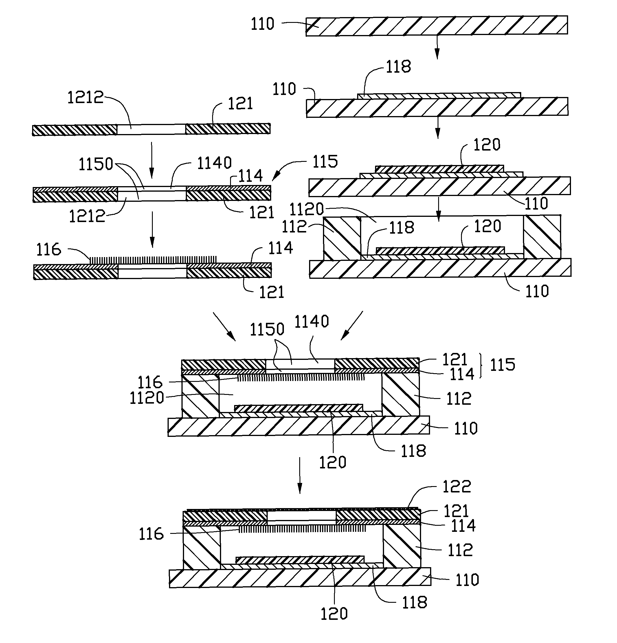
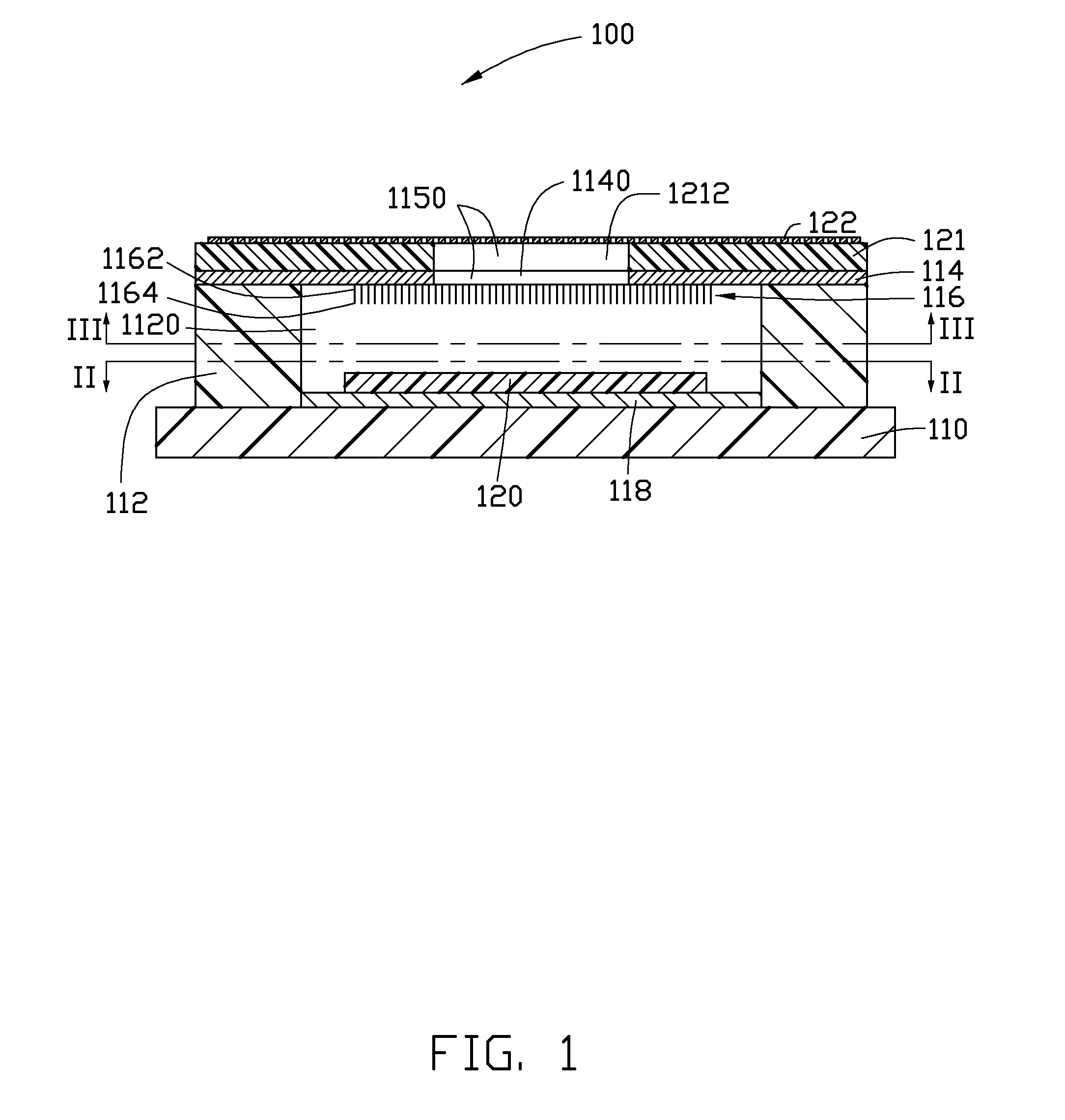
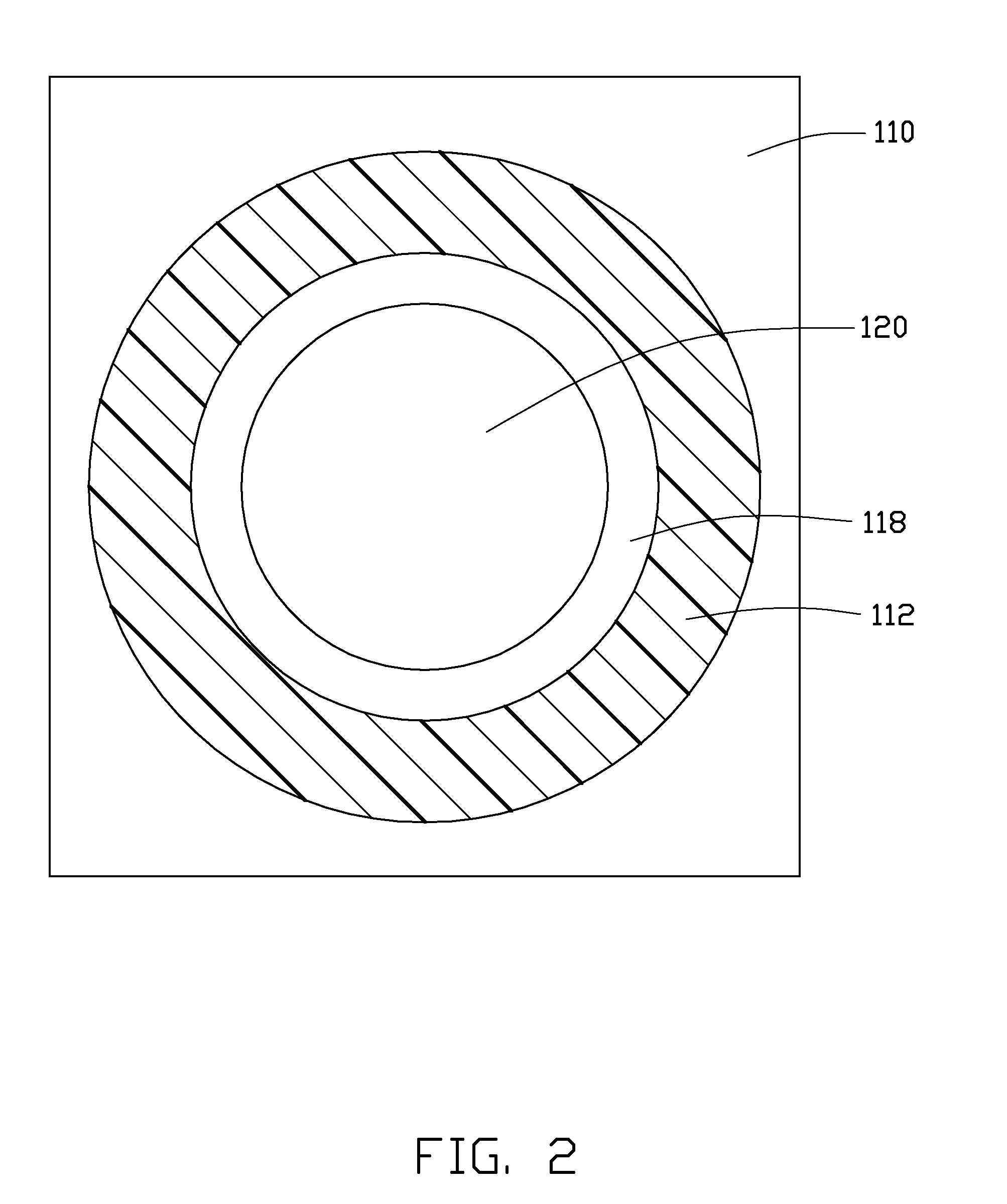
[0022]Referring to FIGS. 1 to 3, a field emission device 100 of one embodiment includes an insulative substrate 110, a first dielectric layer 112, a cathode electrode 114, an electron emission layer 116, an electron pulling electrode 118, a secondary electron emission layer 120, a second d...


PUM


Abstract

A method for making a field emission device includes the following steps. An insulative substrate is provided. An electron pulling electrode is formed on the insulative substrate. A secondary electron emission layer is formed on the electron pulling electrode. A first dielectric layer is fabricated. The first dielectric layer has a second opening to expose the secondary electron emission layer. A cathode plate having an electron output portion is provided. An electron emission layer is formed on part surface of the cathode plate. The cathode plate is placed on the first dielectric layer. The electron output portion and the second opening have at least one part overlapped, and at least one part of the electron emission layer is oriented to the secondary electron emission layer via the second opening.

Description

RELATED APPLICATIONS[0001]This application claims all benefits accruing under 35 U.S.C. §119 from China Patent Application No. 201010178171.5, filed on May 20, 2010 in the China Intellectual Property Office, the contents of which are hereby incorporated by reference. This application is related to applications entitled, “FIELD EMISSION DEVICE”, filed on Dec. 3, 2010 with U.S. patent application Ser. No. 12 / 959,592; and “ION SOURCE”, filed on Dec. 3, 2010 with U.S. patent application Ser. No. 12 / 959,601.BACKGROUND[0002]1. Technical Field[0003]The present disclosure relates to a field emission device, a method for making the same, and an ion source using the same.[0004]2. Description of Related Art[0005]Field emission displays (FEDs) are a new, rapidly developing flat panel display technology.[0006]Field emission devices are important elements in FEDs. A field emission device usually includes an insulating substrate, a cathode electrode located on the insulating substrate, a dielectri...

Claims


Application Information

Patent Timeline
Patent Type & Authority Patents(United States)
IPC IPC(8): H01J1/00
CPCH01J1/304H01J1/32H01J3/021H01J9/025H01J9/125
Inventor LIU, PENGZHOU, DUAN-LIANGCHEN, PI-JINHU, ZHAO-FUGUO, CAI-LINDU, BING-CHUFAN, SHOU-SHAN
Owner TSINGHUA UNIV
Why Eureka
Try Eureka