
Method of forming semiconductor patterns

a semiconductor pattern and pattern technology, applied in semiconductor/solid-state device manufacturing, basic electric elements, electric devices, etc., can solve the problems of difficult control of the uniform amount of shrinking of such a photo resist shrink step or trimming step, higher and collapsing of photo resist lines, so as to reduce the amount of pr footing and reduce the chance of patterning failure. , the effect of increasing the trimming ra

Active Publication Date: 2012-08-28
ASM KOREA LTD
View PDF4 Cites 382 Cited by
  • Summary
  • Abstract
  • Description
  • Claims
  • Application Information

AI Technical Summary

Benefits of technology

"The invention aims to solve problems in a trimming step used in a process of depositing a spacer oxide. The invention provides a method to perform trimming simultaneously with the deposition of the spacer oxide using a Plasma Enhanced Atomic Layer Deposition process. This method reduces PR footing during the trimming process. The invention also includes a method to perform a two-step process of PR trimming under direct plasma and deposition of SiO2 film to further reduce PR footing."

Problems solved by technology

If the target Critical Dimension of lines is getting smaller than 30 nm, it will become difficult to control the uniformity of the amount of shrinking of such a photo resist shrink step or trimming step.
Furthermore, there is a higher chance of patterning failure due to the leaning or collapsing of photo resist line due to the weak footing of the photo resist line when the photo resist line becomes narrower by the trimming.

Method used


Image

  • Method of forming semiconductor patterns
  • Method of forming semiconductor patterns
  • Method of forming semiconductor patterns

Examples


experimental example 1

[0037]A SiO2 film deposition by PEALD on photo resist template patterns is carried out with the following conditions.

[0038]Metalorganic precursors or halosilane precursors containing Si can be used as Si precursors. In the present invention, for example, SiH2[N(C2H5)2]2 was used as a Si precursor. Susceptor temperature for heating substrate varied from room temperature to 200 degree C., preferably the susceptor temperature was 50 degree C. During deposition, process pressure is maintained in a range from 1 to 10 Torr, preferably at a value of about 3 Torr. RF plasma power is in a range from 10 to 1000 W, preferably at a value of about 200 W.

[0039]Gas flow condition is as follows.[0040]Source Ar flow rate for carrying bubbled precursor into reactor: 200 sccm[0041]Temperature of precursor container: 60° C.[0042]O2 reactant flow rate: 50 sccm[0043]Reactant Ar flow rate for flowing into reactor with oxygen: 200 sccm[0044]Main Ar flow rate for chamber / gas line purge: 200 sccm

[0045]Proces...

experimental example 2

[0051]A SiO2 film deposition by PEALD on photo resist template patterns is carried out with the following conditions.

[0052]Metalorganic precursors or halosilane precursors containing Si can be used as Si precursors. In this invention, SiH2[N(C2H5)2]2 was used as a Si precursor. Susceptor temperature for heating substrate varied from room temperature to 200 degree C., preferably the susceptor temperature was 50 degree C. During deposition, process pressure is maintained in a range from 1 to 10 Torr, preferably at a value of about 3 Torr. RF plasma power is in a range from 10 to 1000 W, preferably at a value of about 100 W to 150 W.

[0053]Gas flow condition:[0054]Source Ar flow rate for carrying bubbled precursor into reactor: 500 sccm[0055]Temperature of precursor container: 60° C.[0056]O2 reactant flow rate: 1000 sccm[0057]Reactant Ar flow rate for flowing into reactor with oxygen: 500 sccm[0058]Main Ar flow rate for chamber / gas line purge: 200 sccm[0059]Reaction space gap between sh...


PUM


Abstract

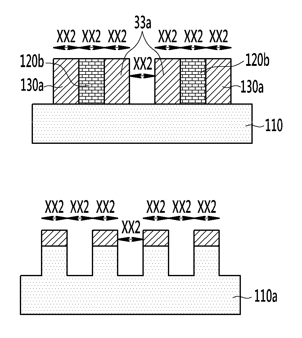
Semiconductor patterns are formed by performing trimming simultaneously with the process of depositing the spacer oxide. Alternatively, a first part of the trimming is performed in-situ, immediately before the spacer oxide deposition process in the same chamber in which the spacer oxide deposition is performed whereas a second part of the trimming is performed simultaneously with the process of depositing the spacer oxide. Thus, semiconductor patterns are formed reducing PR footing during PR trimming with direct plasma exposure.

Description

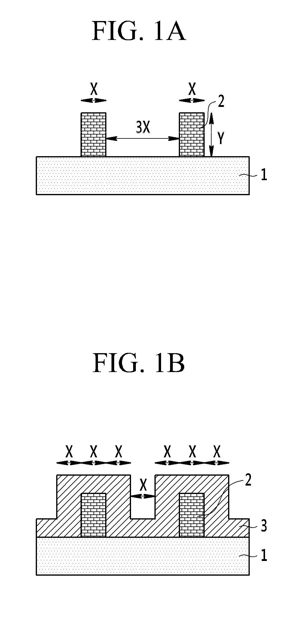
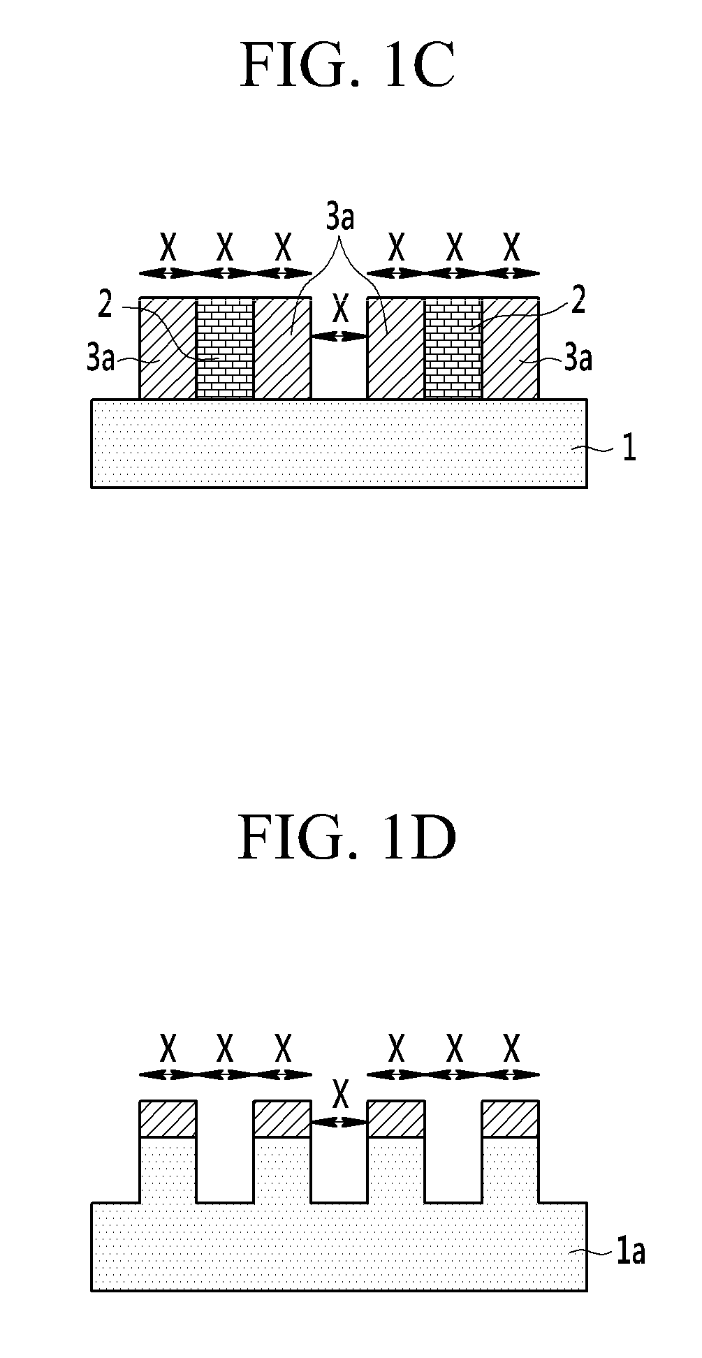
CROSS-REFERENCE TO RELATED APPLICATIONS[0001]This application claims the benefit of U.S. Provisional Application No. 61 / 323,918, filed on Apr. 14, 2010, in the United States Patent and Trademark Office, the disclosure of which is incorporated herein in its entirety by reference.BACKGROUND OF THE INVENTION[0002](a) Field of the Invention[0003]The present invention relates to a method of forming semiconductor patterns. More specifically, the present invention relates to a spacer defined double patterning (SDDP) process using a PEALD spacer oxide deposition process having trimming action.[0004](b) Description of the Related Art[0005]Due to the limit of resolution of the immersion ArF lithography, the method of Double Patterning is used in the chip patterning process for 3× nm half pitch and below.[0006]In the art, the method of Spacer Defined Double Patterning, as represented in FIGS. 1A-1D, is as follows. As shown in FIG. 1A, photo resist template patterns 2 are formed on top of a bot...

Claims


Application Information

Patent Timeline
Patent Type & Authority Patents(United States)
IPC IPC(8): H01L21/311
CPCH01L21/02222H01L21/0337H01L21/0228H01L21/02274H01L21/0274
Inventor BEYNET, JULIENPARK, HYUNG SANGINOUE, NAOKI
Owner ASM KOREA LTD
Learn More