Light emitting diode device

a technology of light-emitting diodes and led lamps, which is applied in the direction of fibre light guides, lighting and heating apparatus, light source combinations, etc., can solve the problems of uneven light distribution and shadowing effect, unsatisfactory vertical light-emitting applications, and uneven light distribution to the bottom or side, etc., to achieve good heat-sinking properties, low loss, and wide beam angle

Inactive Publication Date: 2012-09-04
SHARP KK
View PDF33 Cites 35 Cited by
  • Summary
  • Abstract
  • Description
  • Claims
  • Application Information

AI Technical Summary

Benefits of technology

[0013]The present invention provides an LED device with low loss, wide beam angle and good heat-sinking properties. In addition, the invention provides an inexpensive method of volume manufacturing. The LED device includes a waveguide, and a light extraction and redistribution region positioned at an elevated height from the metal heat-sink chassis on top of the waveguide. The LED device preferably uses a clear glass casing in this case.
[0014]An aspect of the invention is for the point of light source to be elevated to a position above a surface mounted LED, away from the metal-heat sink chassis. This in turn allows light to be distributed in an isotropic manner, and light directed downwards is not shielded by the heat-sink chassis, essentially creating a wider beam angle.

Problems solved by technology

While the LED narrow beam angle property makes LED bulbs ideal for down-lighting applications (mounted on ceiling), it is not ideal for vertical-lighting applications, whereby light is not distributed to the bottom or sides well enough.
This results in uneven light distribution and shadowing effect.
Conventional methods of using diffusive coating on an LED dome casing to increase scattering and subsequently the beam angle typically results in light loss of 20-30%, resulting in reduced emission efficiency.
Increasing the metal heat-sink area will increase the total LED bulb size and weight, making the light bulb design poorer and less appealing to consumers.
Although the beam angle is increased from FIG. 1A, the uniformity of light intensity distribution is poor, and the angular distribution very different to a CFL bulb.
The diffusive coating 4 is a source of light loss, reducing the LED bulb efficiency.
In this configuration, heat-sinking of LEDs is not optimal, since the LEDs are not directly mounted onto a heat-sink.
The complexity of mounting LEDs in this manner will also increase manufacturing costs.
Therefore the method described in this citation will be limited to low power LEDs.
Good heat-sinking is difficult to achieve in this method, since the LEDs are only in direct contact with a small area of the heat-sink.
This method will also be difficult to implement for an LED bulb using a single LED instead of multiple LEDs.
This method can produce a wider beam angle LED device, but will create a dark spot directly above it, which results in shadowing effects that are not desirable.
This method is not suitable for single module LED bulbs and manufacturing costs will also be higher compared to bulbs with LEDs mounted directly on the heat-sink chassis.
This is a consequence of the complexity of the mounting geometry of the proposed configuration.
Although this invention describes an enhanced light angular distribution, the optical device used is very complex and would be difficult to manufacture cheaply.
This is important since cost is a key issue for LED device to be competitive against conventional incandescent and CFL lamps.

Method used


Image

  • Light emitting diode device
  • Light emitting diode device
  • Light emitting diode device

Examples


embodiment 1

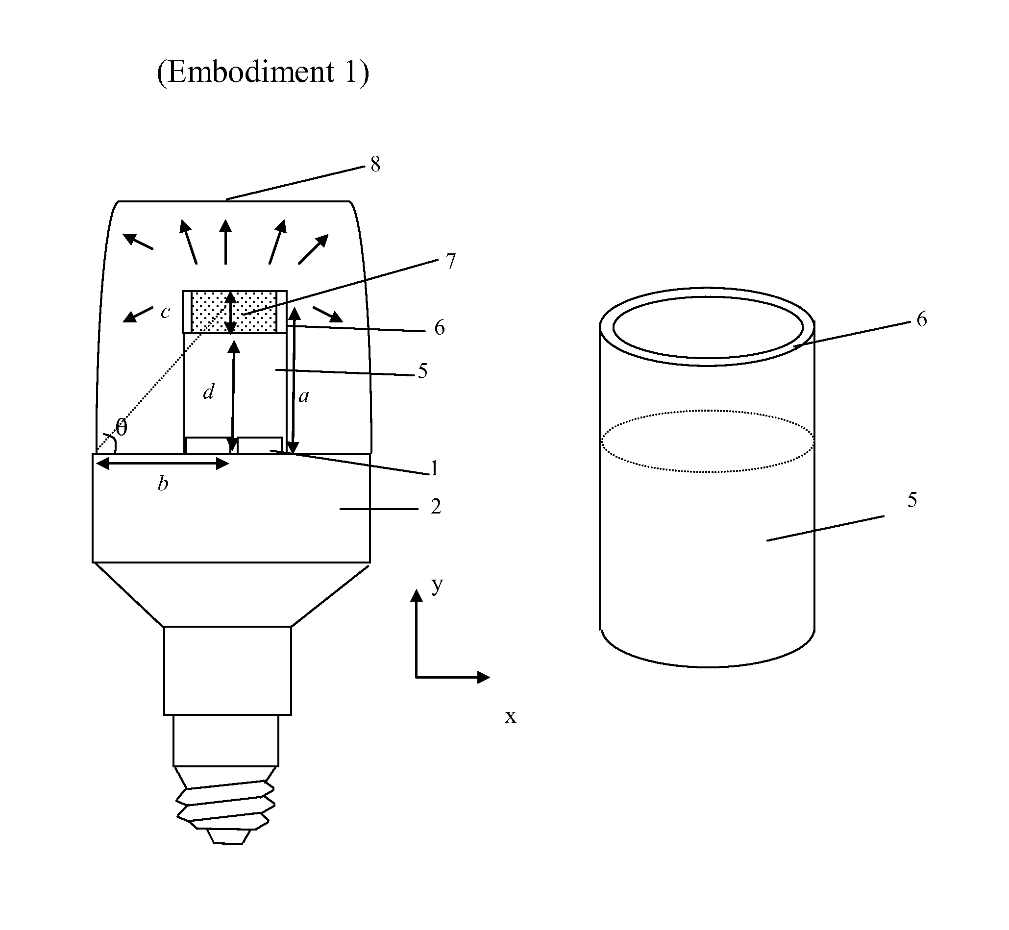
[0063]A first particular embodiment of an LED device in accordance with the present invention is illustrated in FIG. 9A. The LED device includes one or more LEDs 1, a metal heat-sink chassis 2, a waveguide 5 with a pocket region 6 created at the top of the waveguide 5, and a light extraction and redistribution region 7. The waveguide unit 5 acts to elevate the point of light source from the LED 1 to the light extraction and redistribution region 7, to overcome light emitted downwards from being shielded by the metal heat-sink chassis 2. The waveguide 5 can be made from any known light guide materials with minimal optical absorption, and in this example, clear polished acrylic is used. In the exemplary embodiments described herein, the LED device is an LED bulb including a conventional screw-type mount 25 for mounting the bulb in a conventional screw-type socket of the type included in consumer lamps, etc. It will be appreciated, however, that the LED device may also be any of a vari...

embodiment 2

[0067]According to this embodiment, the general structure in FIG. 8 can be modified to the structure shown in FIG. 10A. For this structure, the acrylic waveguide 5 is similarly used to elevate the point of light source. However, in this embodiment the light extraction and redistribution region is made up of holes 10 formed in the top region of the waveguide 5 (an example is shown in inset of FIG. 10A). The holes 10 will reflect and refract the light in all directions. Indeed the difference in refractive index between the waveguide material and air is large enough to create optical reflection when light hits the interface between the waveguide 5 and air. The manner that the holes 10 are positioned in the waveguide 5 can be tailored to realise different types of angular light distribution patterns as will be appreciated by those having ordinary skill in the art. This method is beneficial because the entire waveguide 5 and light redistribution region made up by the holes 10 is easy to ...

embodiment 3

[0069]According to Embodiment 3 of the invention, the structure in FIG. 8 can be modified as shown in FIG. 11. For this structure, the acrylic waveguide 5 is similarly used to elevate the point of light source to the light redistribution region. In this case, the light distribution region is made of a partially transmitting mirror 11. The partially transmitting mirror 11 is formed at the top of the waveguide 5 such that it will transmit a certain percentage of the light and reflect / refract a certain percentage that is directed to it. In this case, the partially transmitting mirror 11 will reflect and refract some light downwards and sideways, but also allow some light to be distributed upwards.

[0070]The partially transmitting mirror 11 can be made of a thin metal layer, or more preferably be made of materials with different refractive indices to reduce loss / absorption, deposited on the top surface of the waveguide 5. As shown in FIG. 11, the partially transmitting mirror 11 may incl...


PUM


Abstract

A light emitting diode device which includes at least one light emitting diode, a heat-sink chassis having a surface upon which the at least one light emitting diode is mounted, and a waveguide having one end coupled to the at least one light emitting diode for receiving light therefrom. The waveguide has another end which includes a light extraction and redistribution region, and the waveguide is configured to guide light received from the at least one light emitting diode away from the heat-sink chassis and towards the light extraction and redistribution region. The light extraction and redistribution region is configured to extract and redistribute the light from the waveguide.

Description

TECHNICAL FIELD OF THE INVENTION[0001]The present invention relates to a light emitting diode (LED) device, and in particular an LED device such as an LED bulb having a wide angular light distribution. A method of volume manufacturing such a device with low cost and low absorption loss is also presented.BACKGROUND OF THE INVENTION[0002]Light emitting diodes are gaining popularity to be used as light sources for various applications. Since the demonstration of high quality Gallium Nitride crystal growth, high efficiency Indium Gallium Nitride quantum well blue LED chips emitting at around 450 nm (blue) wavelength have been intensely developed worldwide. White LED chips obtained from phosphor converted blue LEDs are now used in general lighting and backlighting applications. In particular, LED bulbs are being developed as replacement lamps for incandescent bulbs, halogen bulbs, cold cathode fluorescent lamps (CCFL) and compact fluorescent lamps (CFL) for general lighting applications....

Claims


Application Information

Patent Timeline
Patent Type & Authority Patents(United States)
IPC IPC(8): H01L33/48H01L33/58H01L33/60
CPCF21K9/135F21K9/1355F21K9/52F21K9/56F21V3/00G02B6/0008F21K9/58F21Y2105/001F21Y2101/02F21Y2113/005F21Y2105/10F21K9/23F21K9/232F21K9/61F21K9/64F21K9/65F21Y2115/10F21Y2113/13
Inventor TAN, WEI-SINBERRYMAN-BOUSQUET, VALERIEZHANG, TONGHEFFERNAN, JONATHAN
Owner SHARP KK
Why Eureka
Try Eureka