Loop filter and phase locked loop including the same

a phase locked loop and loop filter technology, applied in the field of loop filters, can solve the problems of reducing the phase margin of the phase locked loop, increasing the chip area and chip cost, and about a 20% error rate, and achieve the effect of reducing the chip area

Active Publication Date: 2012-09-04
ELECTRONICS & TELECOMM RES INST
View PDF9 Cites 5 Cited by
  • Summary
  • Abstract
  • Description
  • Claims
  • Application Information

AI Technical Summary

Benefits of technology

[0015]An aspect of the present invention provides a loop filter and a phase locked loop including the same, which are capable of reducing chip area and achieving on-chip integration by replacing a charge pump and a first capacitor having a large element value included in a conventional loop filter with a dual charge pump, a first capacitor having a small element value, and an operational amplifier.
[0016]An aspect of the present invention also provides a loop filter and a phase locked loop including the same, which are capable of obtaining an optimal phase margin even though process and temperature are changed when it is integrated.

Problems solved by technology

First, the capacitor having a capacitance of 1 nF or more occupies a large chip area when it is integrated. When assuming that the capacitance corresponding to 1 μm2 is 1 nF, an integrated circuit area of 1 mm2 is required when 1-nF capacitance is implemented by using a metal-insulator-metal (MIM) capacitor. This may cause an increase in chip areas and chip costs.
Second, the element values of the passive elements inside the loop filter have about a 20% error rate due to variations in process and temperature when they are integrated. This may seriously degrade a phase margin of a phase locked loop.
However, the open chip design may increase costs of individual frequency mixer parts due to an increase in number of chip resistors, chip capacitors, and wire bondings.

Method used


Image

  • Loop filter and phase locked loop including the same
  • Loop filter and phase locked loop including the same
  • Loop filter and phase locked loop including the same

Examples


Embodiment Construction

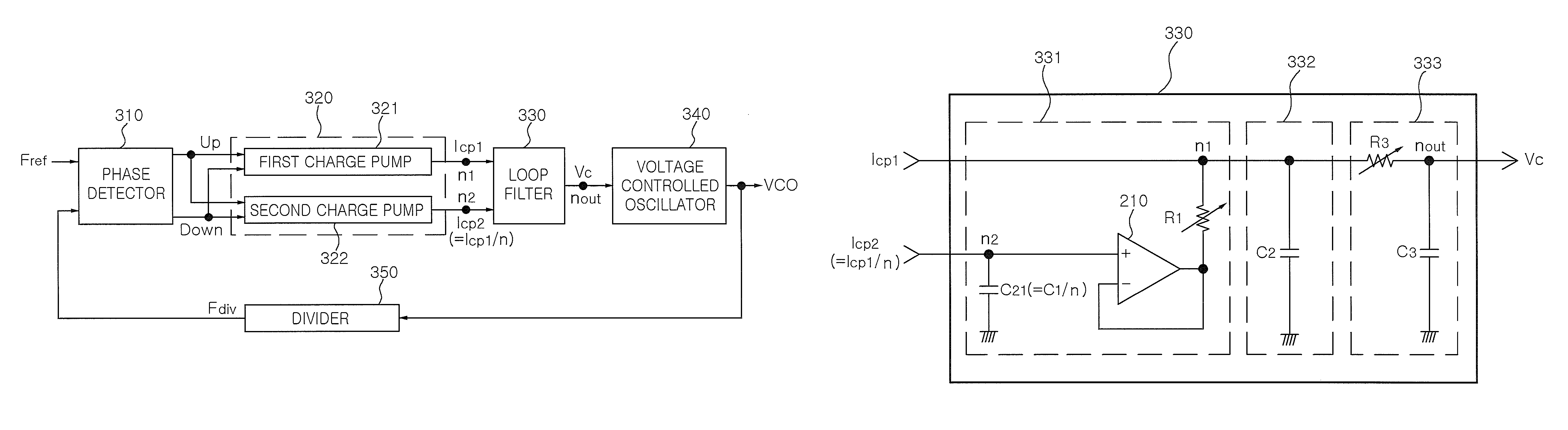
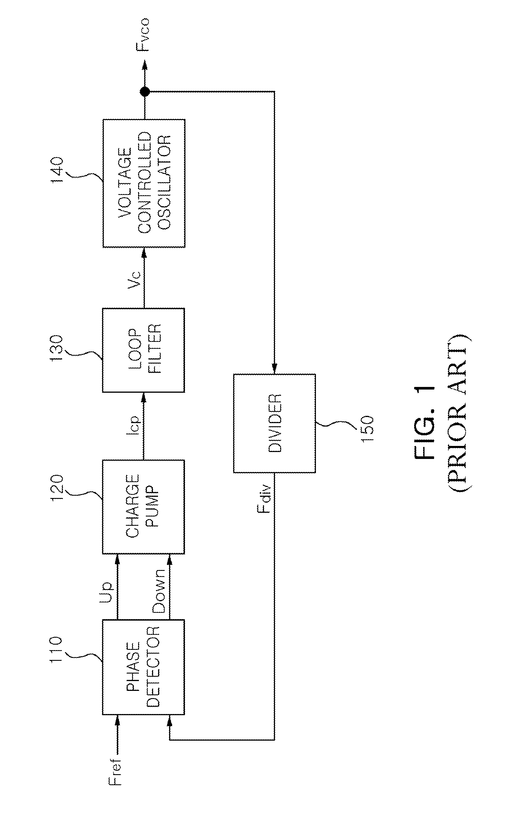
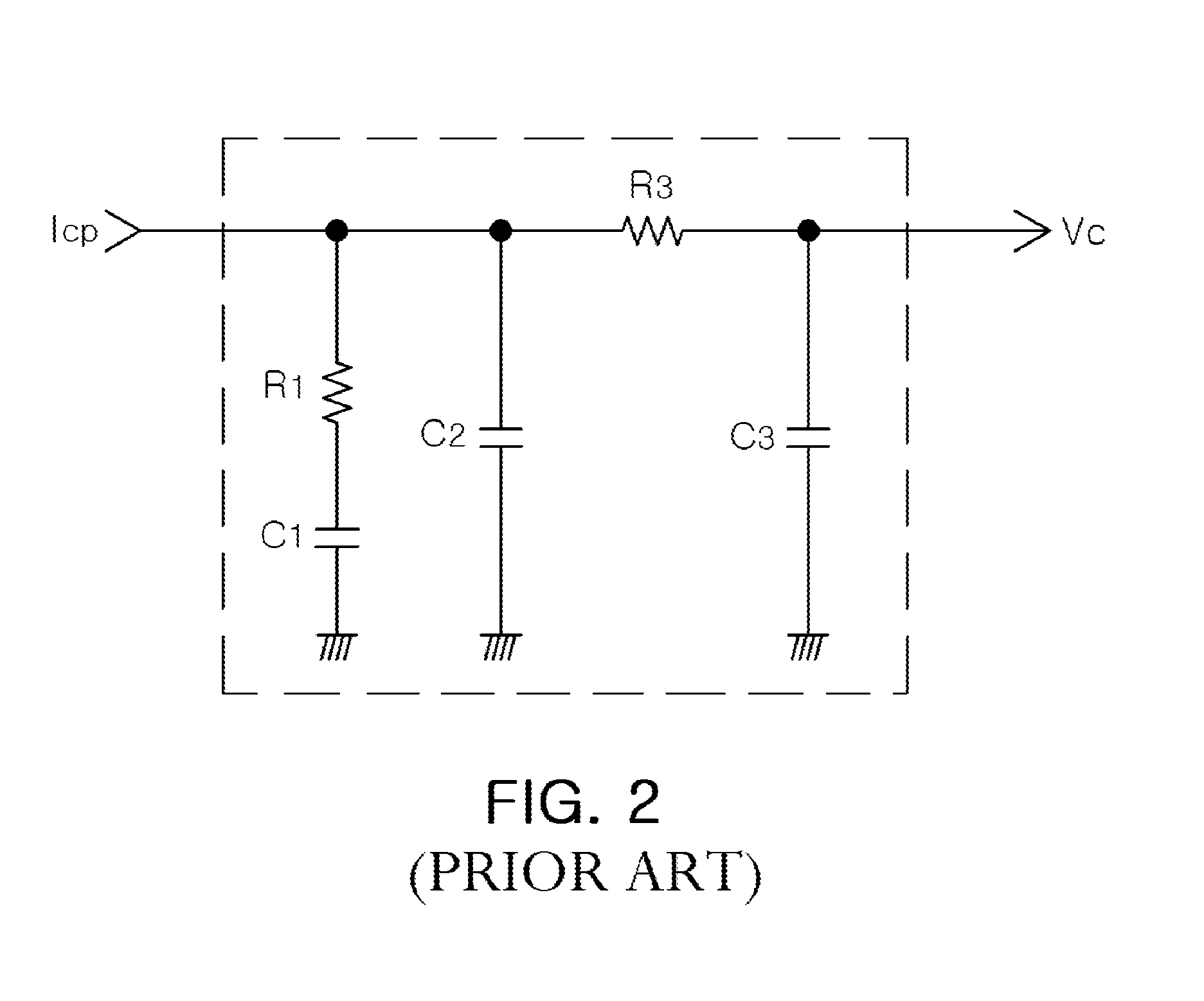
[0039]Exemplary embodiments of the present invention will now be described in detail with reference to the accompanying drawings. The invention may, however, be embodied in many different forms and should not be construed as being limited to the embodiments set forth herein. Rather, these embodiments are provided so that this disclosure will be thorough and complete, and will fully convey the scope of the invention to those skilled in the art. In the drawings, the thicknesses of layers and regions are exaggerated for clarity. Like reference numerals in the drawings denote like elements, and thus their description will be omitted.

[0040]It will be understood that when an element is referred to as being “connected to” another element, it can be directly connected to the other element or intervening elements may also be present. In contrast, when an element is referred to as being “directly connected to” another element, there are no intervening elements present. In addition, unless exp...


PUM


Abstract

Provided is a loop filter which receives first and second currents whose current ratio is n (where n is a natural number). The loop filter includes a first-order filter path, a second-order filter path, and a third-order filter path. The first-order filter path includes an operational amplifier generating an output impedance by increasing by as much as n times an impedance of a second input node to which the second current is applied. The first-order filter path performs a first-order filtering on the first current applied to a first input node by using the operational amplifier. The second-order filter path performs a second-order filtering on the first current applied to the first input node. The third-order filter path performs a third-order filtering on the first current applied to the first input node.

Description

CROSS-REFERENCE TO RELATED APPLICATIONS[0001]This application claims the priority of Korean Patent Application No. 10-2009-0111880 filed on Nov. 19, 2009, in the Korean Intellectual Property Office, the disclosure of which is incorporated herein by reference.BACKGROUND OF THE INVENTION[0002]1. Field of the Invention[0003]The present invention relates to a loop filter for the on-chip integration of a frequency mixer, and more particularly, to a loop filter and a phase locked loop including the same, which are capable of reducing chip area by 50% or more, while providing the same performance as the existing capacitor, by replacing a high-capacitance capacitor being a passive element with a low-capacitance capacitor and an operational amplifier in designing a third-order loop filter for a phase locked loop of a frequency mixer.[0004]2. Description of the Related Art[0005]Frequency mixers are widely used to generate stable frequencies for transmission / reception in the fields of mobile c...

Claims


Application Information

Patent Timeline
Patent Type & Authority Patents(United States)
IPC IPC(8): H03L7/06
CPCH03L7/093H03L7/0893H03L7/08
Inventor MIN, BYUNG HUN
Owner ELECTRONICS & TELECOMM RES INST
Why Eureka
Try Eureka