Technique for modeling parasitics from layout during circuit design and for parasitic aware circuit design using modes of varying accuracy

a technology of layout and parasitic effects, applied in error detection/correction, program control, instruments, etc., can solve the problems of rf and high-performance analog designs being extremely sensitive to layout parasitic effects, affecting the electrical behavior of rf and high-performance analog designs, and shortening the typical analog/mixed-signal methodology described abov

Active Publication Date: 2012-09-04
CADENCE DESIGN SYST INC
View PDF18 Cites 43 Cited by
  • Summary
  • Abstract
  • Description
  • Claims
  • Application Information

AI Technical Summary

Problems solved by technology

Radio frequency (RF) and High-Performance Analog designs are extremely sensitive to layout parasitic effects.
Since RF and high-performance analog designs however are extremely sensitive to layout parasitics, the typical analog/mixed-signal methodology described above falls short because the final extracted design may not meet the design specifications and will often require a re-design and re-layout.
Additionally, the electrical behavior of RF and high-performance analog designs is increasingly being affected by layout intricacies, forcing designers to account for these effects early in the design cycle.
For most designs, the circuit may not meet all the specifications in the presence of layout parasitics, which are only detected after layout extraction, once the layout is complete.
The existing approaches to estimate parasitics early in the design have been mostly manual and limited to parasitic estimation on the schematic.
This approach is limited to analyzing parasitics estimated on the schematic.
It does not offer any support for fetching parasitic in

Method used


Image

  • Technique for modeling parasitics from layout during circuit design and for parasitic aware circuit design using modes of varying accuracy
  • Technique for modeling parasitics from layout during circuit design and for parasitic aware circuit design using modes of varying accuracy
  • Technique for modeling parasitics from layout during circuit design and for parasitic aware circuit design using modes of varying accuracy

Examples


Embodiment Construction

Overview

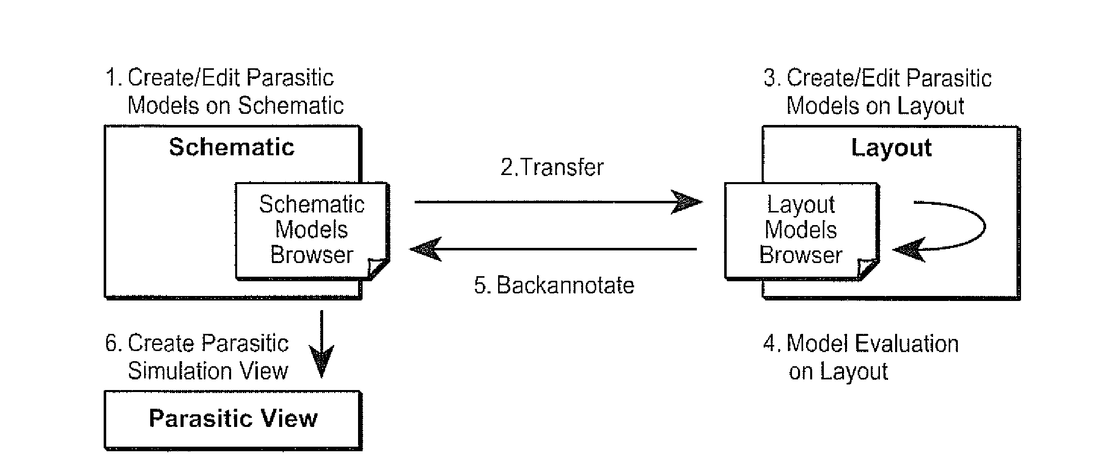
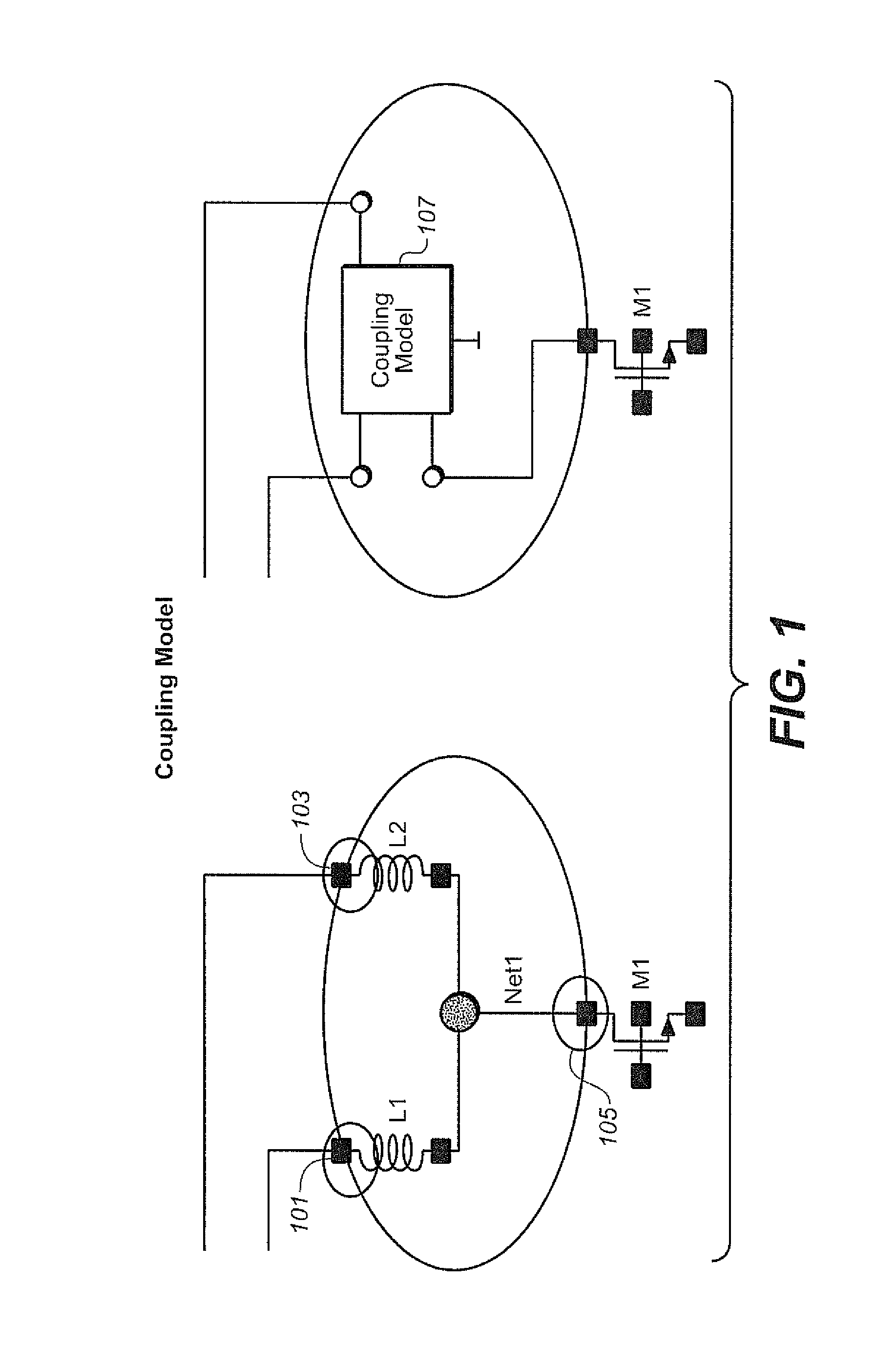
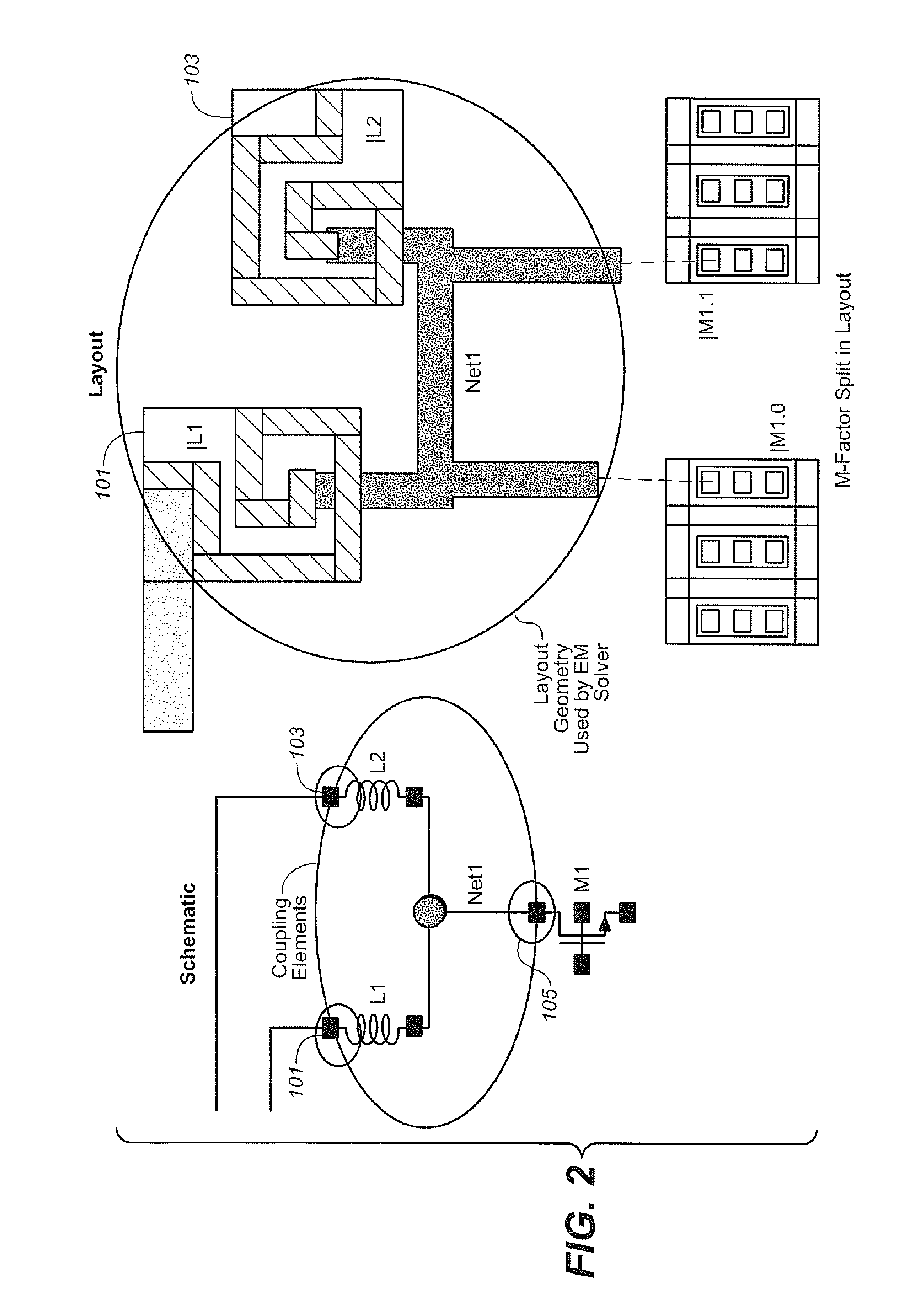
[0026]As discussed in the Background, the electrical behavior of RF (radio frequency) and high-performance analog designs is increasingly being affected by layout intricacies that force designers to account for these effects early in the design cycle. Current analog / mixed-signal design flows are largely manual, relying on separate front-end design by a designer, who sizes the circuit schematic to meet performance goals, followed by hand-off to a layout engineer who places and routes the design. For most designs, the circuit may not meet all the specifications in the presence of layout parasitics, which are only detected after layout extraction once the layout is complete, resulting in multiple iterations between sizing and layout. To mitigate this problem, designers need to account for parasitics early in the design cycle, during circuit design and layout.

[0027]While some early estimation of parasitics is possible by using simplistic equation-based approximation techniques, ...


PUM


Abstract

Techniques are presented for accounting for parasitics in the automated design of integrated circuits. In one set of techniques, model values for parasitic models are received on a schematic environment from a user, the parasitic models are evaluated from the schematic using the received model values, the parasitic models are transferred to a layout environment, and the transferred parasitic models are evaluated on the layout environment. In other techniques, model values are received for parasitic models from a user, the parasitic models are evaluated on the layout environment, and the process then backannotates the parasitic models evaluated on the layout environment and corresponding parameter values to a schematic environment. In yet other techniques, a user is presented with a simulation environment within which the user is provided a choice to select between parasitic simulation modes of varying accuracy, the modes including a mode without parasitics and a plurality of modes including parasitics with a varying degree of accuracy. A selection from among the modes is received from the user and simulation test are performed at the selected degree of accuracy.

Description

BACKGROUND OF THE INVENTION[0001]1. Field of Invention[0002]This invention relates generally to techniques for treating parasitics in the design of integrated circuits. More specifically, it presents techniques that allow the design process to be aware of parasitics with varying degree of accuracy and also techniques allowing parasitics to be modeled during circuit design from the layout.[0003]2. Description of Related Art[0004]Radio frequency (RF) and High-Performance Analog designs are extremely sensitive to layout parasitic effects. With increased manufacturability challenges and aggressive performance goals, these parasitic effects are preferably taken into account early in the design cycle, during the circuit sizing and optimization process.[0005]In a typical analog and mixed signal design methodology, the designer starts by designing the circuit in the absence of parasitics. At this point, the simulation tests point to the original schematic. Once the simulation outputs meet t...

Claims


Application Information

Patent Timeline
IPC IPC(8): G06F17/50
CPCG06F17/5036G06F17/5081G06F30/367G06F30/398
Inventor GOPALAKRISHNAN, PRAKASHYAN, RONGCHANGSHAH, AKSHAT H.DIXON, DAVID N.DENNISON, KEITH
Owner CADENCE DESIGN SYST INC
Why Eureka
Try Eureka