Detection circuit with improved anti-blooming circuit

a detection circuit and anti-blooming technology, applied in the field of detection circuits, can solve problems such as unusability of circuits, and achieve the effect of reliable and repeatable fabrication and easy implementation

Active Publication Date: 2012-09-25
LYNRED
View PDF3 Cites 3 Cited by
  • Summary
  • Abstract
  • Description
  • Claims
  • Application Information

AI Technical Summary

Benefits of technology

[0012]The object of the invention is to provide a detection circuit that corrects blooming phenomena and that is easy to implement while at the same time ensuring a reliable and repeatable fabrication for industrial integration.
[0014]It is a further object of the invention to provide a method for protecting the detection circuit that is easy to implement while at the same time ensuring a reliable and repeatable fabrication for industrial integration.

Problems solved by technology

The circuit proposed in the document US 2003 / 0034433 provides a theoretical answer to the general problem of the blooming phenomenon, but this circuit is not satisfactory as the constraints that bear on an industrial use of this architecture are too numerous and make this circuit unusable from an industrial point of view.

Method used


Image

  • Detection circuit with improved anti-blooming circuit
  • Detection circuit with improved anti-blooming circuit
  • Detection circuit with improved anti-blooming circuit

Examples


Embodiment Construction

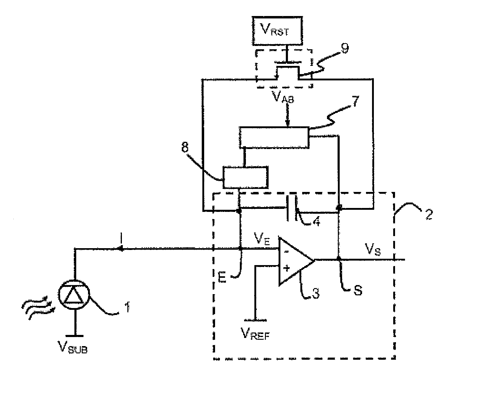
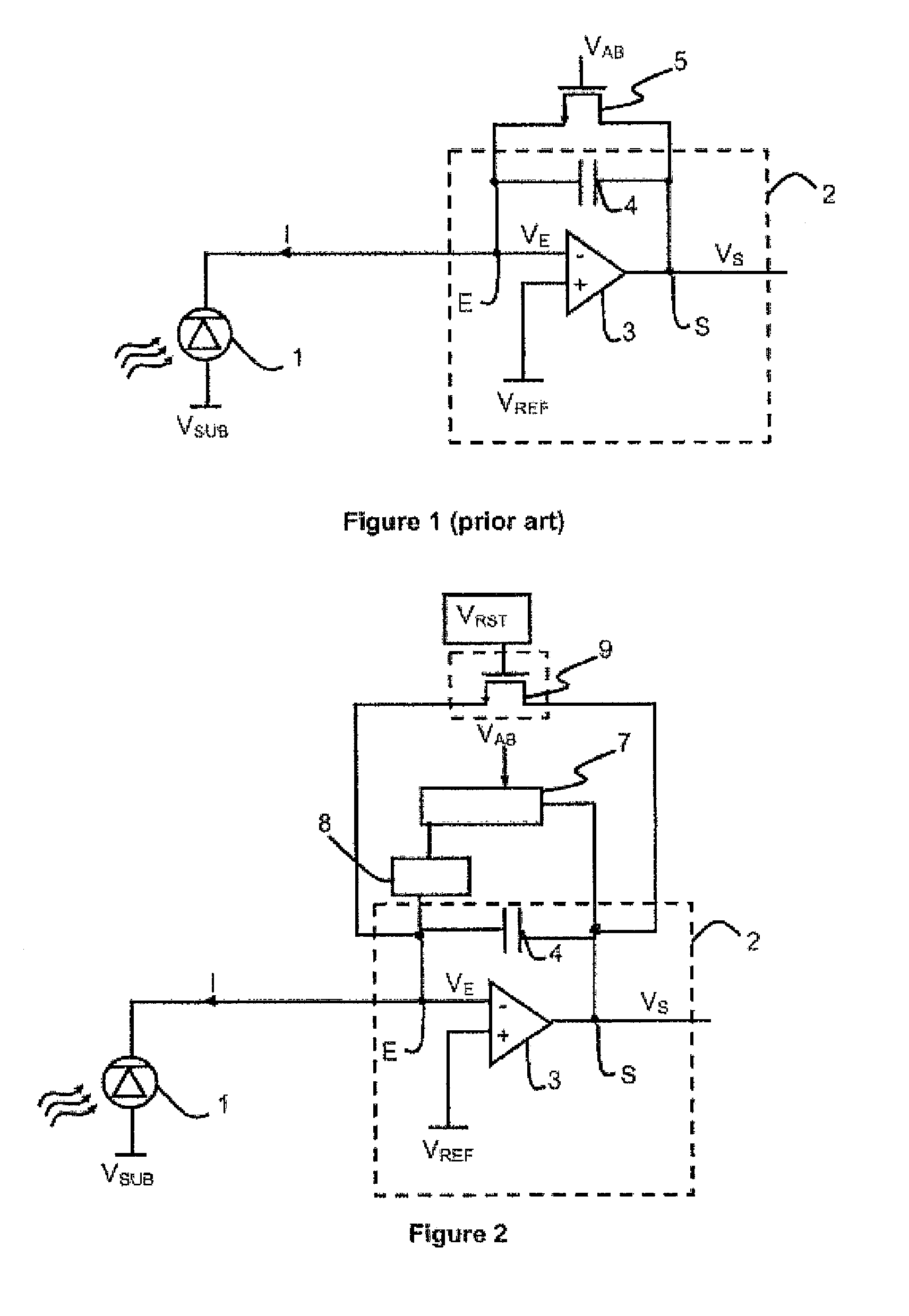
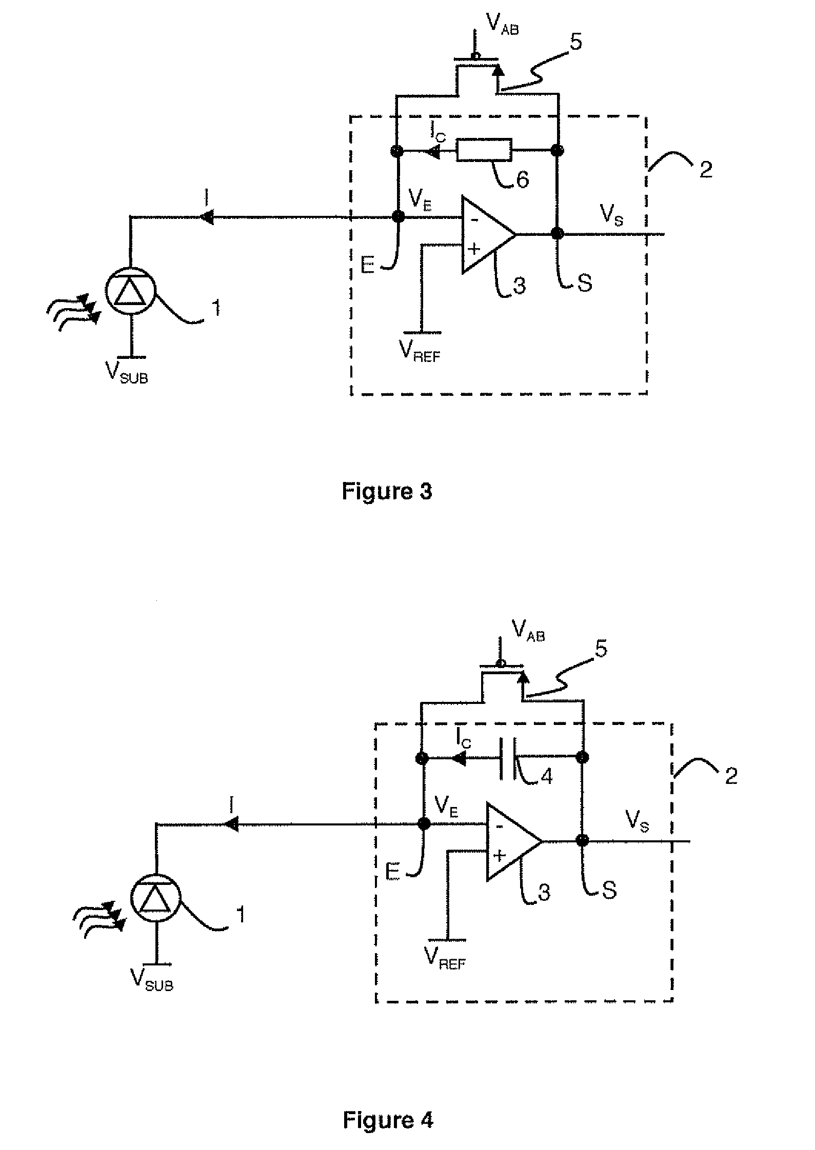
[0024]In the circuit according to the prior art illustrated in FIG. 1, nMOS transistor 5 connected in parallel to the terminals of capacitor 4 has to prevent a blooming phenomenon from occurring on the adjacent photodiodes. Transistor 5 therefore has to prevent photodiode 1 from changing bias, but it must not however prevent capacitor 4 from storing a minimum of charges necessary for the foremost purpose of the detection circuit which is to define the lighting of the observed scene. It is apparent from these two conditions that the anti-blooming voltage VAB applied to the gate electrode of nMOS transistor 5 has to be comprised within a precise range.

[0025]According to the first condition, anti-blooming voltage VAB applied to the gate electrode of nMOS transistor 5 has to be lower than the reference voltage VREF applied to the second input of amplifier 3 to which the threshold voltage Vth of transistor 5 is added. In this way, nMOS transistor 5 is not permanently conducting, as volta...


PUM


Abstract

The detection circuit comprises a photodiode connected to an input of a capacitive transimpedance amplifier. The circuit comprises an anti-blooming circuit connected between the input and an output of the capacitive transimpedance amplifier. The anti-blooming circuit comprises a field effect transistor connected between the input and output of the capacitive transimpedance amplifier. The transistor is of pMOS type when the input of the capacitive transimpedance amplifier is connected to a cathode of the photodiode. The transistor is of nMOS type when the input of the capacitive transimpedance amplifier is connected to an anode of the photodiode.

Description

BACKGROUND OF THE INVENTION[0001]The invention relates to a detection circuit comprising:[0002]a photodiode connected to an input of a transimpedance amplifier,[0003]an anti-blooming circuit connected between the input and an output of the transimpedance amplifier.[0004]The invention also relates to a method for reading the radiation of a detection circuit.STATE OF THE ART[0005]As illustrated in FIG. 1, in conventional detection circuits, a reverse biased photodiode 1 delivers a current representative of an observed scene. Photodiode 1 delivers this current to an integrator device 2 during a pre-defined period.[0006]Integrator device 2 is formed by a capacitive transimpedance amplifier which comprises an amplifier 3 connected to a capacitor 4. The cathode of photodiode 1 is connected to a first input of amplifier 3 and a substrate voltage VSub is applied to the anode of photodiode 1. So long as the voltage of the first input of amplifier 3 is higher than substrate voltage VSub, the ...

Claims


Application Information

Patent Timeline
Patent Type & Authority Patents(United States)
IPC IPC(8): H03F3/08
CPCG01J1/46H04N5/3591H04N25/621
Inventor BAUD, LAURENT
Owner LYNRED
Why Eureka
Try Eureka