Organic light emitting diode display

a light-emitting diode and organic light-emitting technology, applied in the field of display, can solve the problems of difficult to adopt the transistor as the switch transistor and the drive transistor, the back-channel effect affecting the characteristics of the transistor, and the difficulty in forming a high-quality insulating film, so as to achieve excellent off-state characteristics, swing characteristics, and saturation characteristics.

Active Publication Date: 2012-10-02
SAMSUNG DISPLAY CO LTD +1
View PDF20 Cites 5 Cited by
  • Summary
  • Abstract
  • Description
  • Claims
  • Application Information

AI Technical Summary

Benefits of technology

[0013]An etch-stopper thin film transistor in which an etch stopper layer which is a silicon nitride film (SiNx film) or the like is provided above the laminated film including the high-crystallinity semiconductor layer and the low-crystallinity semiconductor layer is provided as a conventional technology which prevents overetching of the laminated film. Because the overetching of the laminated film which occurs in the dry etching is prevented by the etch stopper layer, only the ohmic contact film may be selectively removed, which enables prevention of the damage to the laminated film. However, because the etch stopper layer is formed after the laminated film is formed, it is difficult to form a high-quality insulating film, and a large amount of fixed charge is formed in the etch stopper layer. Therefore, the fixed charge in the etch stopper layer may cause the back-channel effect, and it affects the transistor characteristics, for example, the off-state characteristics, the swing characteristics, or the saturation characteristics may be degraded, or the threshold voltage may be shifted to be smaller voltage.
[0014]The present invention has been made in view of the above-mentioned circumstance, and an object of the present invention is to provide an organic light emitting diode display which may suppress a back-channel effect.
[0021]According to the present invention, the thin film transistor used in the organic light emitting diode display which has excellent off-state characteristics, swing characteristics, and saturation characteristics may be attained.

Problems solved by technology

Because the active semiconductor layer is damaged by the overetching, a back-channel effect may occur and the back-channel effect affects transistor characteristics.
If such a phenomenon occurs, it is difficult to adopt the transistor as the switch transistor and the drive transistor used in the pixel circuit of the current-driven display, in particular, the organic light emitting diode display.
However, because the etch stopper layer is formed after the laminated film is formed, it is difficult to form a high-quality insulating film, and a large amount of fixed charge is formed in the etch stopper layer.

Method used


Image

  • Organic light emitting diode display
  • Organic light emitting diode display
  • Organic light emitting diode display

Examples


embodiment 1

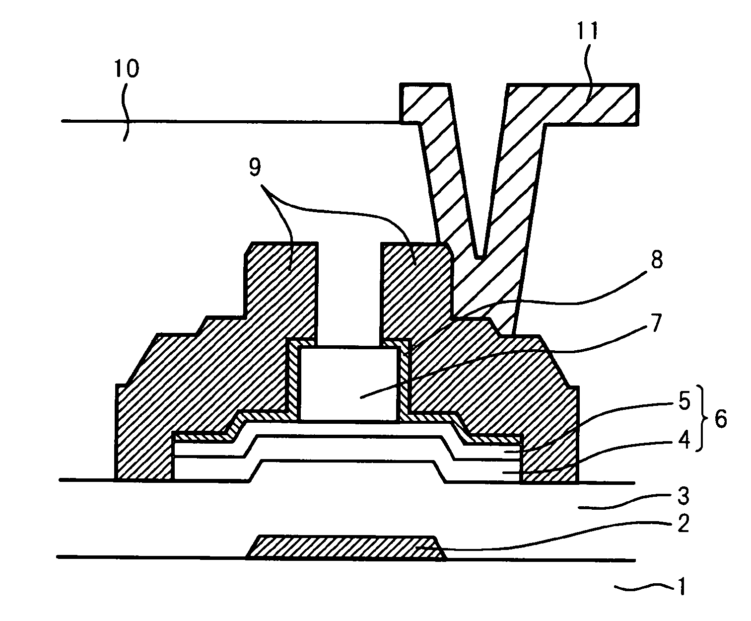
[0048]FIG. 5 illustrates an organic light emitting diode display 200 according to Embodiment 1 of the present invention. As illustrated in FIG. 5, the organic light emitting diode display 200 includes an upper frame 210 and a lower frame 220 for fixing by sandwiching an OLED panel which includes a thin film transistor substrate 100 and an encapsulating substrate (not shown), a circuit board 240 including a circuit element for generating information to be displayed, and a flexible substrate 230 for conveying to the thin film transistor substrate 100 display information of RGB generated in the circuit board 240.

[0049]FIG. 6 illustrates a structure of a circuit of the thin film transistor substrate 100 of the organic light emitting diode display 200 illustrated in FIG. 5. As illustrated in FIG. 6, as a basic structure, the thin film transistor substrate 100 includes on the substrate 1a data driver 101, a selection scanning driver 102, a power supply scanning driver 103, and a display r...

embodiment 2

[0059]FIG. 9 illustrates sectional views of respective manufacturing process steps of a thin film transistor 25 of an organic light emitting diode display according to Embodiment 2 of the present invention. It is to be noted that the structure of the organic light emitting diode display in which the thin film transistor is used is similar to those of the organic light emitting diode display 200 illustrated in FIG. 5 and of the thin film transistor substrate 100 illustrated in FIGS. 6 and 7 according to Embodiment 1, therefore, description thereof is omitted.

[0060]A method of manufacturing the thin film transistor 25 according to this embodiment is characterized in that, after the source / drain electrodes 9 are patterned, part of the ohmic contact film 8 on the active semiconductor layer 6 is plasma oxidized to form the back channel protection insulating film 7. It is to be noted that part of description of this embodiment which is similar to that of Embodiment 1 is omitted.

[0061]Firs...

embodiment 3

[0066]FIG. 10 illustrates sectional views of respective manufacturing process steps of a thin film transistor 35 of an organic light emitting diode display according to Embodiment 3 of the present invention. It is to be noted that the structure of the organic light emitting diode display in which the thin film transistor 35 is used is similar to those of the organic light emitting diode display 200 illustrated in FIG. 5 and of the thin film transistor substrate 100 illustrated in FIGS. 6 and 7 according to Embodiment 1, therefore, description thereof is omitted.

[0067]FIG. 10 illustrates sectional views of respective manufacturing process steps of the thin film transistor 35 according to Embodiment 3 of the present invention. A method of manufacturing the thin film transistor 35 according to this embodiment is characterized in that the number of photolithography steps necessary for the manufacture may be reduced and still the on-state characteristics is excellent. It is to be noted t...


PUM


Abstract

An organic light emitting diode display includes a thin film transistor on a substrate (1). The thin film transistor includes a gate electrode (2), a gate insulating film (3) that covers the gate electrode (2), a first semiconductor film (4) provided on the gate insulating film (3), a second semiconductor film (5) provided on the first semiconductor film (4), a back channel protection insulating film (7) and an ohmic contact film (8) provided on the second semiconductor film (5), and source / drain electrodes (9). A crystallinity of the first semiconductor film (4) is higher than that of the second semiconductor film (5). The back channel protection insulating film (7) is formed as one of an organic insulating film and an organic / inorganic hybrid insulating film. The thin film transistor has excellent off-state characteristics, swing characteristics, and saturation characteristics.

Description

CROSS-REFERENCE TO RELATED APPLICATION[0001]The present application claims priority from Japanese application JP2009-223265 filed on Sep. 28, 2009, the content of which is hereby incorporated by reference into this application.BACKGROUND OF THE INVENTION[0002]1. Field of the Invention[0003]The present invention relates to a display, and more particularly, to an organic light emitting diode (OLED) display using thin film transistors.[0004]2. Description of the Related Art[0005]In recent years, the displays using an organic light emitting diode which consists of thin organic films with electroluminescence (EL) in each pixel receive attention as a next generation flat panel display to replace a liquid crystal display. The display, that is, an organic light emitting diode display referred to as OLED display, is different from the conventional liquid crystal display in that, because of the self-emission phenomenon, an additional light source is not necessary, which enables decrease in vo...

Claims


Application Information

Patent Timeline
Patent Type & Authority Patents(United States)
IPC IPC(8): H01L33/02
CPCH01L29/04H01L29/66765H01L29/78696H01L27/3262H10K59/1213
Inventor ASANUMA, HARUHIKOKAWACHI, GENSHIRO
Owner SAMSUNG DISPLAY CO LTD
Why Eureka
Try Eureka