Semiconductor device with lower layer wiring

a technology of mico-layer wiring and mico-layer, which is applied in the direction of transistors, basic electric elements, instruments, etc., can solve the problems of increased leakage current, damage, failure of the entire system, etc., and achieve the effect of reducing the possibility of structural disruption of the mim capacitor and restrainting an increase of leakage curren

Inactive Publication Date: 2012-10-16
RENESAS ELECTRONICS CORP
View PDF3 Cites 0 Cited by
  • Summary
  • Abstract
  • Description
  • Claims
  • Application Information

AI Technical Summary

Benefits of technology

[0014]According to the semiconductor device of the present invention, the lower layer wirings formed underneath the MIM capacitor is not arranged right below the one or more than one edge of the upper electrode whose plane is made rectangular. In this case, layout flexibility of the lower wiring underneath the MIM capacitor is restricted, thus decreasing the occupancy of the lower layer wirings underneath the MIM capacitor.
[0015]As a result, it is possible to decrease the possibility of the structural disruption of the MIM capacitor due to the hillock generation in the lower layer wiring, thus decreasing the possibility of the leakage current, as compared to the general semiconductor device. In the general semiconductor device, a plurality of lower layer wirings are spread with spacing in accordance with the designing standard, underneath the MIM capacitor. There is formed a large enough area for not arranging the lower layer wirings. Thus, it is possible to maintain the sufficient process stability or high integration of the lower wirings.
[0020]According to the method of designing lower layer wirings and the lower layer wiring designing device of the present invention, it is possible to design the lower layer wirings after determining the arrangement position of the MIM capacitor, and it is also possible to determine the arrangement position of the MIM capacitor after designing the lower layer wirings. As a result, it is possible to adequately design the lower layer wirings based on the required performance of the semiconductor device.
[0021]According to the semiconductor device, the lower layer wiring designing device, the method of designing lower layer wirings and the computer program of the present invention, it is possible to decrease the possibility of the structural disruption of the MIM capacitor. As a result, it is possible to restrain an increase of the leakage current.

Problems solved by technology

However, the MIM capacitors may cause a failure of LSI having the MIM capacitors therein or a failure of the entire system due to an increase in leakage current resulting from the structural disruption.
This damage is affected by the process temperatures of the stress of the laminated interlayer film.
This results in an increase in the leakage current.
This may cause a fissure of the capacity dielectric film 220.
In this case, layout flexibility of the lower wiring underneath the MIM capacitor is restricted, thus decreasing the occupancy of the lower layer wirings underneath the MIM capacitor.

Method used


Image

  • Semiconductor device with lower layer wiring
  • Semiconductor device with lower layer wiring
  • Semiconductor device with lower layer wiring

Examples


example 1

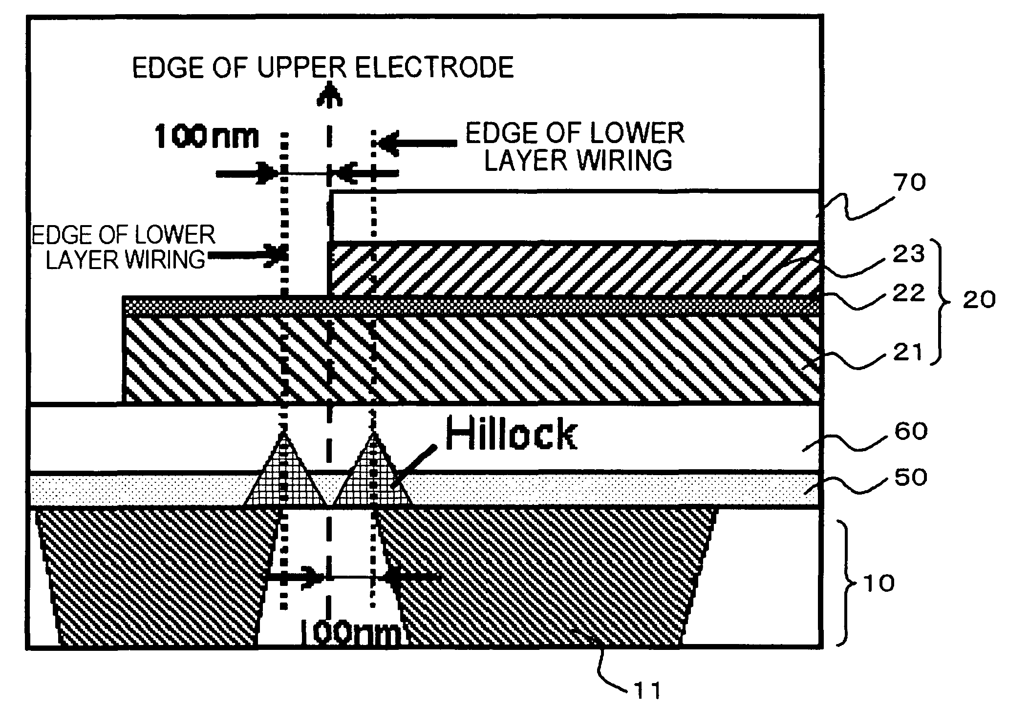
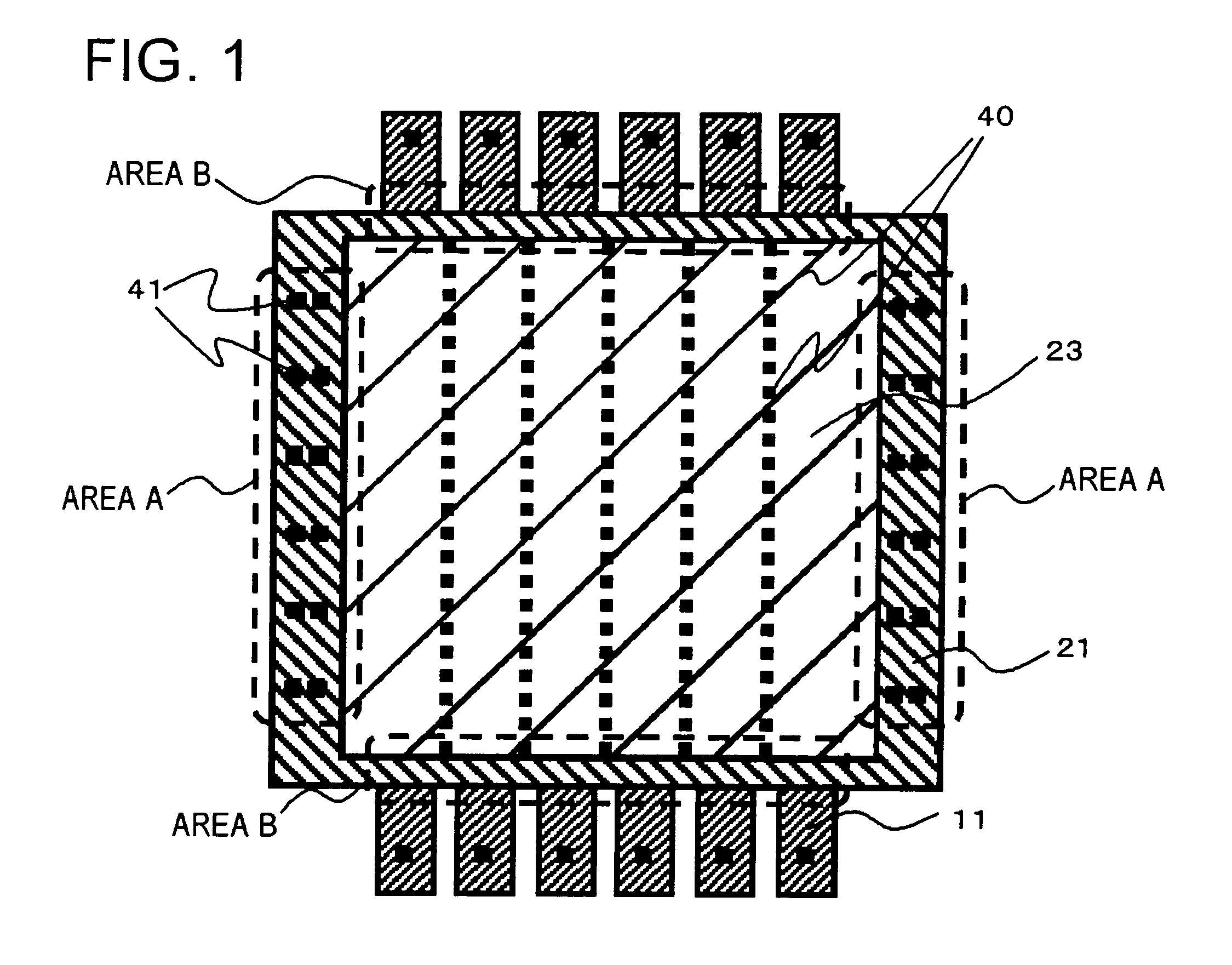
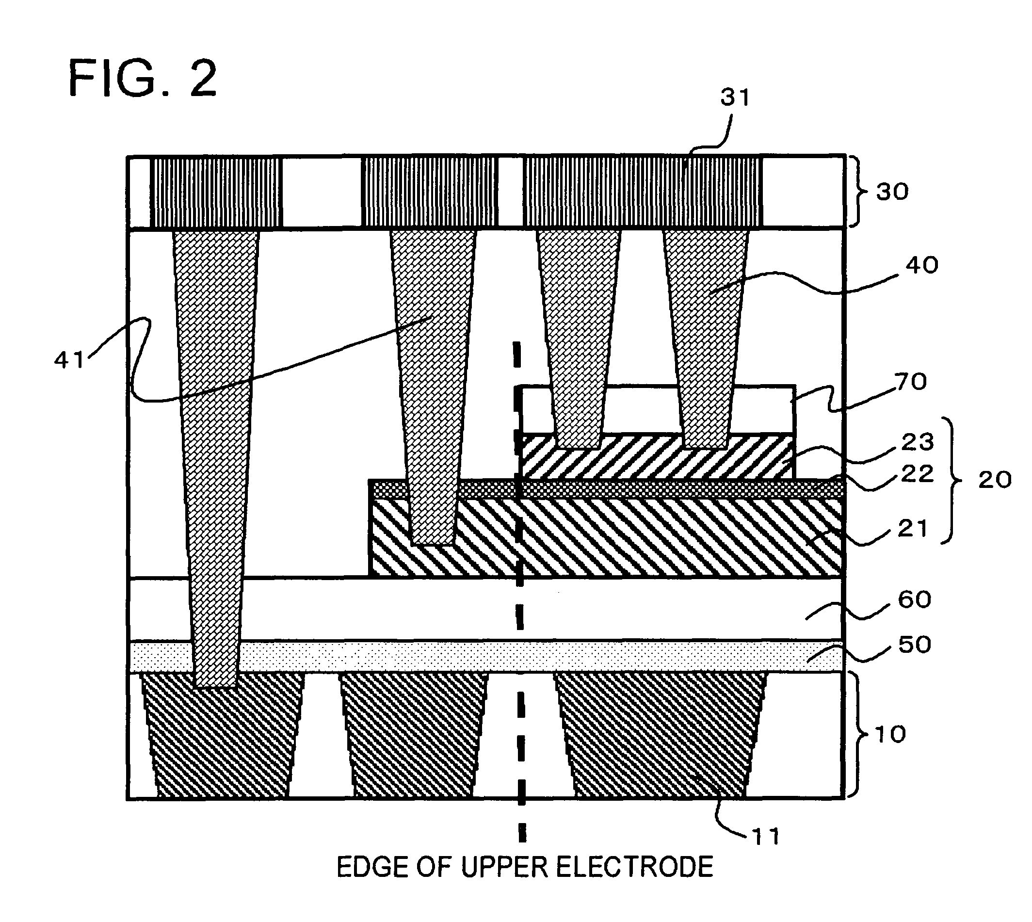
[0064]As shown in a functional block diagram of FIG. 6, an example of the lower layer wiring designing device of this embodiment includes an MIM arrangement position determination unit 1, a lower layer wiring arrangement forbidden area information acquisition unit 2, a lower layer wiring arrangement forbidden area information retention unit 3, a forbidden area consideration designing unit 4 and an output unit 5. The lower layer wiring designing device of this embodiment may store a lower layer wiring arrangement forbidden area specification condition in its internal memory. The lower layer wiring arrangement forbidden area specification condition may be stored in a memory of an external unit. The lower layer wiring arrangement forbidden area information acquisition unit 2 acquires the lower layer wiring arrangement forbidden area specification condition so as to use this condition.

[0065]The MIM arrangement position determination unit 1 is configured so as to determine the arrangemen...

example 2

[0080]As shown in a functional block diagram of FIG. 7, another example of a lower layer wiring designing device of this embodiment includes a lower layer wiring designing unit 6, a lower layer wiring consideration MIM arrangement position determination unit 7, the lower layer wiring arrangement forbidden area information acquisition unit 2, the lower layer wiring arrangement forbidden area information retention unit 3, a compensation rule retention unit 8, a compensation unit 9 and the output unit 5. The device may store the lower layer wiring arrangement forbidden area specification condition in its internal memory. The lower layer wiring arrangement forbidden area information acquisition unit 2 may be configured to use the lower layer wiring arrangement forbidden area specification condition. The lower layer wiring arrangement forbidden area specification condition may be stored in an external memory.

[0081]The lower layer wiring designing unit 6 designs the pattern of the lower l...


PUM


Abstract

A semiconductor device includes a lower layer wiring layer, an MIM capacitors and an upper layer wiring layer. The lower layer wiring layer includes a plurality of lower layer wirings. The MIM capacitor is formed above the lower layer wiring layer. The MIM capacitor includes a lower electrode, a capacity dielectric film and an upper electrode which are layered from underneath in this order. A planar form of the upper electrode is smaller than that of the lower electrode. The upper layer wiring layer includes a plurality of upper layer wirings which are connected to the lower electrode and the upper electrode through via plugs. A plane of the upper electrode is made rectangular. The lower layer wirings are not arranged right below one or more than one edge of the plane of the upper electrode.

Description

[0001]This application is based on Japanese patent application No. 2009-128228, the content of which is incorporated hereinto by reference.BACKGROUND[0002]1. Technical Field[0003]The present invention relates to a semiconductor device, a lower layer wiring designing device, a method of designing lower layer wirings and a computer program.[0004]2. Related Art[0005]In recent years, MIM (Metal Insulator Metal) structures are applied not only to DRAMs (Dynamic Random Access Memory), but also to Decoupling Capacitors, in the field of LSI (Large Scale Integration). The MIM structure as an integrated module of LSI has become increasingly important. Thus, it has been common to mount the MIM structure in LSI.[0006]However, the MIM capacitors may cause a failure of LSI having the MIM capacitors therein or a failure of the entire system due to an increase in leakage current resulting from the structural disruption. Therefore, desired is a technique for restraining an increase in a leakage curr...

Claims


Application Information

Patent Timeline
Patent Type & Authority Patents(United States)
IPC IPC(8): H01L21/02H01L27/108
CPCH01L23/5223H01L27/0207H01L28/60H01L24/19H01L2924/0002H01L2924/00
Inventor IWAKI, TAKAYUKI
Owner RENESAS ELECTRONICS CORP
Why Eureka
Try Eureka