Solid-state imaging device, imaging apparatus, pixel driving voltage adjustment apparatus, and pixel driving voltage adjustment method

a technology of pixel driving voltage and imaging device, which is applied in the direction of color television details, television system details, television systems, etc., can solve problems such as noise generation

Active Publication Date: 2012-10-23
SONY SEMICON SOLUTIONS CORP
View PDF8 Cites 6 Cited by
  • Summary
  • Abstract
  • Description
  • Claims
  • Application Information

AI Technical Summary

Benefits of technology

[0013]There is a need for a scheme which can read out signal charges multiple times by using a plurality of transfer driving voltage levels of a charge transfer unit, thereby obtaining a satisfactory image with a good S / N ratio from a small signal to a large signal without causing saturation, and setting the transfer driving voltage level reliably and appropriately.
[0017]One embodiment of the invention can adopt a scheme in which the setting of the voltage level for the intermediate transfer within the transfer driving voltage level (intermediate voltage setting) is adjusted for each device or use environment. For each device, the saturated charge amount and the intermediate voltage retained charge amount are specified, and the intermediate voltage is set to a suitable level on the basis of the result. Therefore, the setting of the intermediate voltage can approach a theoretical value without depending on the devices or use environment, and thus it is possible to assure that there is no image quality disturbance.

Problems solved by technology

Although details will be described in connection with the embodiments, according to the inventors' experiment and discussion based on the experiment result, it has been found that if the complete transfer charge amount which is read by the complete transfer when charge accumulation has passed after the intermediate transfer is disturbed and information deletion occurs, noise is generated.

Method used


Image

  • Solid-state imaging device, imaging apparatus, pixel driving voltage adjustment apparatus, and pixel driving voltage adjustment method
  • Solid-state imaging device, imaging apparatus, pixel driving voltage adjustment apparatus, and pixel driving voltage adjustment method
  • Solid-state imaging device, imaging apparatus, pixel driving voltage adjustment apparatus, and pixel driving voltage adjustment method

Examples


verification experiment

[Description of Verification Experiment]

[0097]FIG. 3B shows the driving timing of intermediate transfer and complete transfer in the verification experiment. The horizontal axis represents the time. A shutter time (charge accumulation time) of the complete transfer is Tlsh, a readout time of the complete transfer is Tl, a shutter time (charge accumulation time) of the intermediate transfer is Tssh, and a readout time of the intermediate transfer is Ts. The vertical axis represents the number of output electrons (charge amount). The number of saturated electrons (saturated charge amount) is Qs, the number of retained electrons by the intermediate transfer (intermediate retained charge amount) is Qm, the number of electrons to be read by the intermediate transfer (intermediate transfer charge amount) is Qn, and the number of electrons to be read by the complete transfer (complete transfer charge amount) is Ql.

[0098]The accumulation time ratio Tratio of the intermediate transfer charge...

first example

[0132]FIGS. 7A to 7D are diagrams illustrating the second embodiment (second example) of the scheme for adjustment of the intermediate voltage. FIG. 7A is a diagram showing a unit pixel 3 having a 3-TR structure to which the second embodiment (second example) is applied. FIG. 7B is a timing chart illustrating the normal driving timing of the unit pixel 3 having the 3-TR structure shown in FIG. 7A. FIG. 7C is a diagram illustrating the relationship between an area identification signal for identifying a normal pixel area and a retained charge measurement area which are applied to the second embodiment (first example), and a pixel array unit. FIG. 7D is a timing chart illustrating the driving timing of the unit pixel 3 having the 3-TR structure shown in FIG. 7A according to the second embodiment (first example).

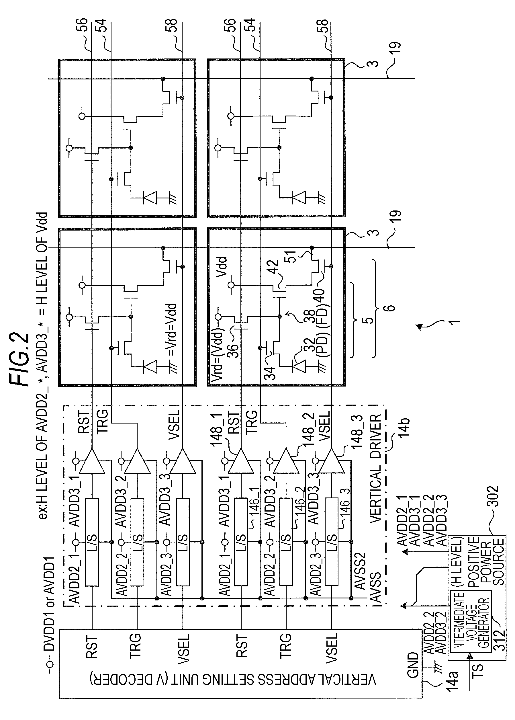
[0133]In the 3-TR structure, the vertical selection transistor 40 in the 4-TR structure is removed. The 3-TR structure is considered to have a feature in that the occupying are...

second example

[0149]FIGS. 8A to 8E are diagrams illustrating the second embodiment (second example) of the scheme for the adjustment of the intermediate voltage. FIG. 8A is a diagram showing a unit pixel 3 having a 4-TR structure to which the second embodiment (second example) is applied. The structure of the unit pixel 3 shown in FIG. 8A is the same as the structure of the unit pixel 3 shown in FIG. 2. FIG. 8B is a diagram showing a structure example of a power source unit 300 which is applied to the second embodiment (second example). FIG. 8C is a diagram illustrating the relationship between the area identification signal Ty for identifying the normal pixel area 10a and the retained charge measurement area 10c which are applied to the second embodiment (second example), the pixel array unit 10, and the pixel power sources Vdd and SELVDD. FIG. 8D is a timing chart illustrating the normal driving timing of the unit pixel 3 having the 4-TR structure shown in FIG. 8A. FIG. 8E is a timing chart ill...


PUM


Abstract

A solid-state imaging device includes: a pixel array unit having arranged unit pixels, each having a charge generator generating signal charges, and a signal output unit having a charge transfer unit, and generating and outputting a processing-target signal corresponding to the signal charges; a driving controller driving the unit pixels, the driving controller sequentially driving the charge transfer unit; and a transfer driving voltage setting unit setting, on the basis of a pixel signal based on a saturated charge amount of the charge generator and a pixel signal based on an intermediate voltage retained charge amount retained in the charge generator after intermediate transfer in which charge transfer is performed at a level between a complete transfer level and an off level, the level of the intermediate voltage such that an actual intermediate voltage retained charge amount becomes the expectation value of the intermediate voltage retained charge amount.

Description

BACKGROUND OF THE INVENTION[0001]1. Field of the Invention[0002]The present invention relates to a solid-state imaging device, an imaging apparatus, a pixel driving voltage adjustment apparatus, and a pixel driving voltage adjustment method. In particular, the present invention relates to a scheme for setting a transfer driving voltage level to a suitable value in a solid-state imaging device which sequentially performs charge transfer at a plurality of different transfer driving voltage levels.[0003]2. Description of the Related Art[0004]In various fields, a semiconductor device (in particular, called a solid-state imaging device) is used which detects signal charges by using a charge generator (a so-called sensor unit, such as a photodiode or the like), which is sensitive to electromagnetic waves from the outside, such as light or radioactive rays, and acquires an image on the basis of an electrical signal (pixel signal) according to the amount of the detected signal charges.[0005...

Claims


Application Information

Patent Timeline
Patent Type & Authority Patents(United States)
IPC IPC(8): H04N5/335H04N5/355H04N5/357H04N5/374H04N5/3745H04N5/376H04N5/378
CPCH04N5/335H04N5/355H04N5/3698H04N25/583H04N25/57H04N25/00H04N25/709
Inventor ITOOIKE, YUSUKE
Owner SONY SEMICON SOLUTIONS CORP
Why Eureka
Try Eureka