
Latency counter, semiconductor memory device including the same, and data processing system

a technology of latch circuits and counters, applied in the field of latch circuits, can solve the problems of increasing the number of latch circuits, and achieve the effects of reducing circuit scale, no power consumption, and reducing output load

Active Publication Date: 2012-10-23
MICRON TECH INC
View PDF8 Cites 6 Cited by
  • Summary
  • Abstract
  • Description
  • Claims
  • Application Information

AI Technical Summary

Benefits of technology

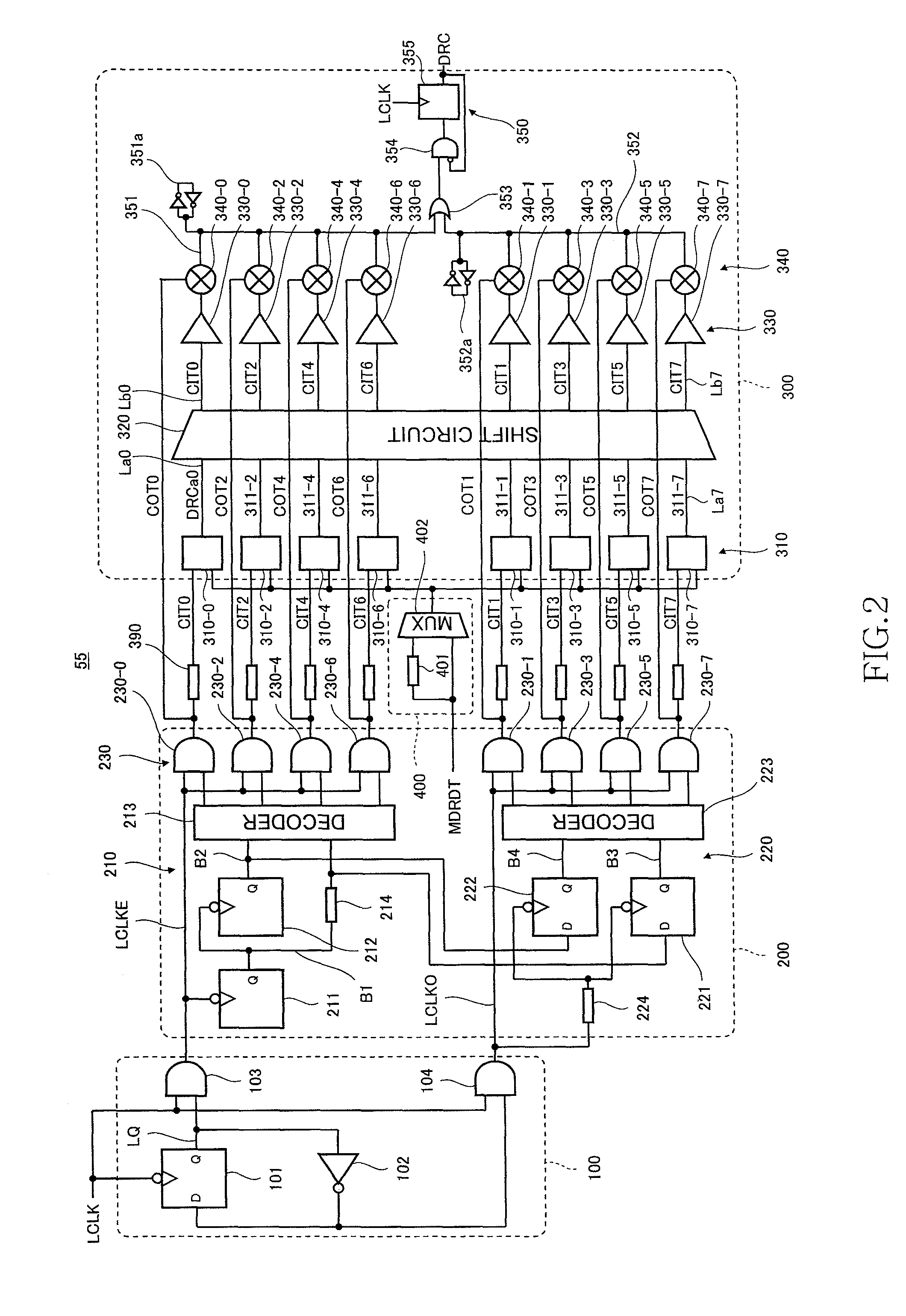
The present invention provides a circuit for reducing latency and power consumption in a data transmission system. The circuit includes a latency counter and a point-shift FIFO circuit. The latency counter counts the time it takes for an internal command to be processed. The point-shift FIFO circuit stores the internal command in a separate circuit and outputs it based on the counter's count. The circuit is designed to reduce the output load and power consumption by dividing the latch circuits into groups and selecting the output of a different group each time the count value is updated. This design also maintains an active level and reduces power consumption during power-up and down cycles.

Problems solved by technology

However, even in the synchronous DRAM, operations performed by the DRAM core are only analog, and therefore it becomes necessary to amplify a very weak electric charge by performing a sense operation.
Consequently, an output load increases with an increase in the number of latch circuits.

Method used


Image

  • Latency counter, semiconductor memory device including the same, and data processing system
  • Latency counter, semiconductor memory device including the same, and data processing system
  • Latency counter, semiconductor memory device including the same, and data processing system

Examples


Embodiment Construction

[0025]Preferred embodiments of the present invention will be explained below in detail with reference to the accompanying drawings.

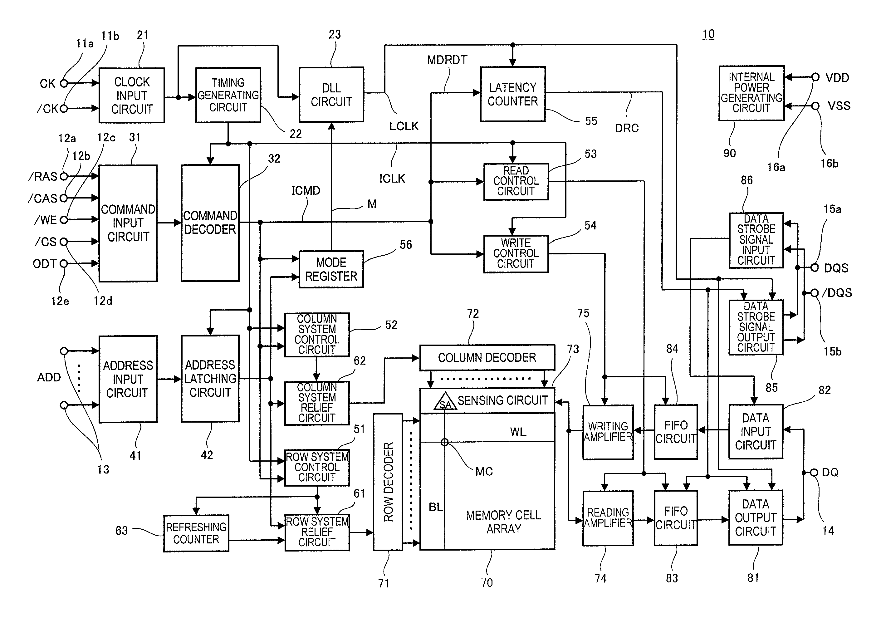
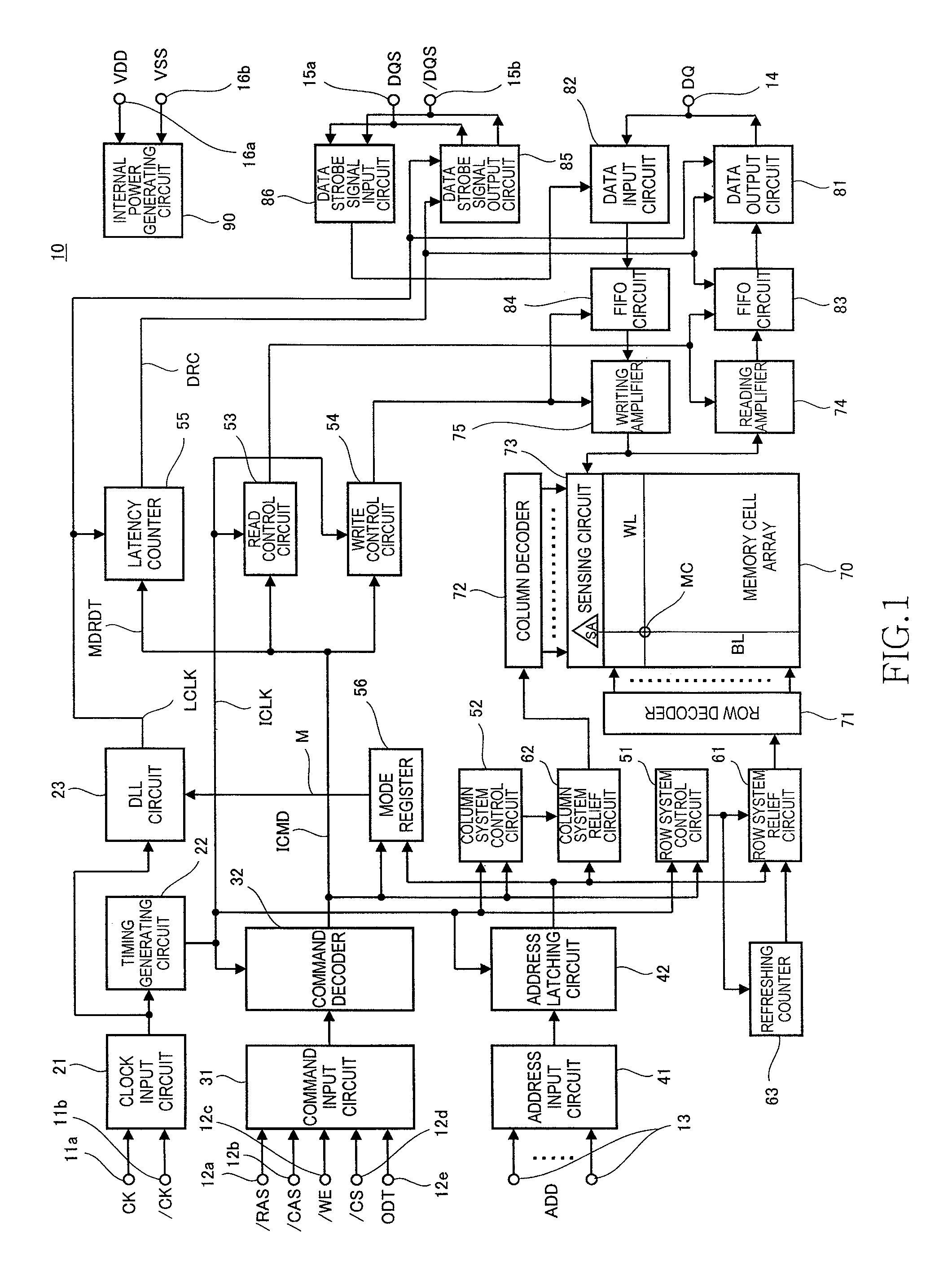
[0026]FIG. 1 is a block diagram showing whole constitution of a semiconductor memory device 10 according to an embodiment of the present invention.

[0027]The semiconductor memory device 10 according to the present embodiment is a synchronous DRAM. The semiconductor memory device 10 includes, as external terminals, clock terminals 11a and 11b, command terminals 12a to 12e, address terminals 13, a data input and output terminal 14, data strobe terminals 15a and 15b, and power terminals 16a and 16b.

[0028]The clock terminals 11a and 11b are terminals to which clock signals CK and / CK are supplied, respectively. These clock signals CK and / CK are then supplied to a clock input circuit 21. In this specification, a signal with a “ / (slash)” at the beginning of the signal name means that the signal is an inverse signal or a low-active signal of a corresponding si...


PUM


Abstract

A latency counter includes a counter circuit and a point-shift FIFO circuit. Latch circuits included in the point-shift FIFO circuit are divided into n groups having wired-OR outputs, and an output of a latch circuit that belongs to a group different from a current group is selected each time a count value is updated.

Description

BACKGROUND OF THE INVENTION[0001]1. Field of the Invention[0002]The present invention relates to a latency counter, and more particularly relates to a latency counter that counts a latency of an internal command within a synchronous memory. The present invention also relates to a semiconductor memory device including the latency counter, and a data processing system including the semiconductor memory device.[0003]2. Description of Related Art[0004]A synchronous memory represented by a synchronous DRAM (Dynamic Random Access Memory) is widely used for a main memory of a personal computer or the like. Because the synchronous memory can input and output data in synchronization with a clock signal supplied from a controller, a data transfer rate can be increased by using a faster clock.[0005]However, even in the synchronous DRAM, operations performed by the DRAM core are only analog, and therefore it becomes necessary to amplify a very weak electric charge by performing a sense operatio...

Claims


Application Information

Patent Timeline
Patent Type & Authority Patents(United States)
IPC IPC(8): G11C8/00
CPCG11C11/4076G11C11/4094G11C2207/2272
Inventor FUJISAWA, HIROKI
Owner MICRON TECH INC
Learn More