
Methods to avoid laser anneal boundary effect within BSI CMOS image sensor array

a technology of image sensor array and laser anneal, which is applied in the field of methods for fabricating image sensors, can solve the problems of laser beams typically not having a uniform distribution of energy across beam width, degraded performance, and decreased sensitivity

Active Publication Date: 2012-11-06
TAIWAN SEMICON MFG CO LTD
View PDF1 Cites 5 Cited by
  • Summary
  • Abstract
  • Description
  • Claims
  • Application Information

AI Technical Summary

Benefits of technology

The present patent describes methods for laser annealing wafers and image sensors with a laser beam. The methods involve determining the size of the laser beam and the desired overlap between scan paths or laser shots. The laser beam is then aligned to not overlap any sensor array region or image sensor. The methods allow for efficient laser annealing of the wafers and image sensors by scanning and shifting the laser beam in a pattern. The technical effects of the methods include improved laser annealing efficiency and reduced likelihood of damage to the wafers and image sensors during the process.

Problems solved by technology

However, the presence of the dielectric and metal layers on the front-side may limit the amount of light absorbed by the photodiodes, resulting in decreased sensitivity and degraded performance.
However, laser beams typically do not have a uniform distribution of energy across the beam width.
As a result, a sensor array region may not be uniformly annealed if it overlaps with a boundary of the laser scan pattern.
It also adversely affects image sensor performance by making it more difficult for the sensor array region to detect light.

Method used


Image

  • Methods to avoid laser anneal boundary effect within BSI CMOS image sensor array
  • Methods to avoid laser anneal boundary effect within BSI CMOS image sensor array
  • Methods to avoid laser anneal boundary effect within BSI CMOS image sensor array

Examples


Embodiment Construction

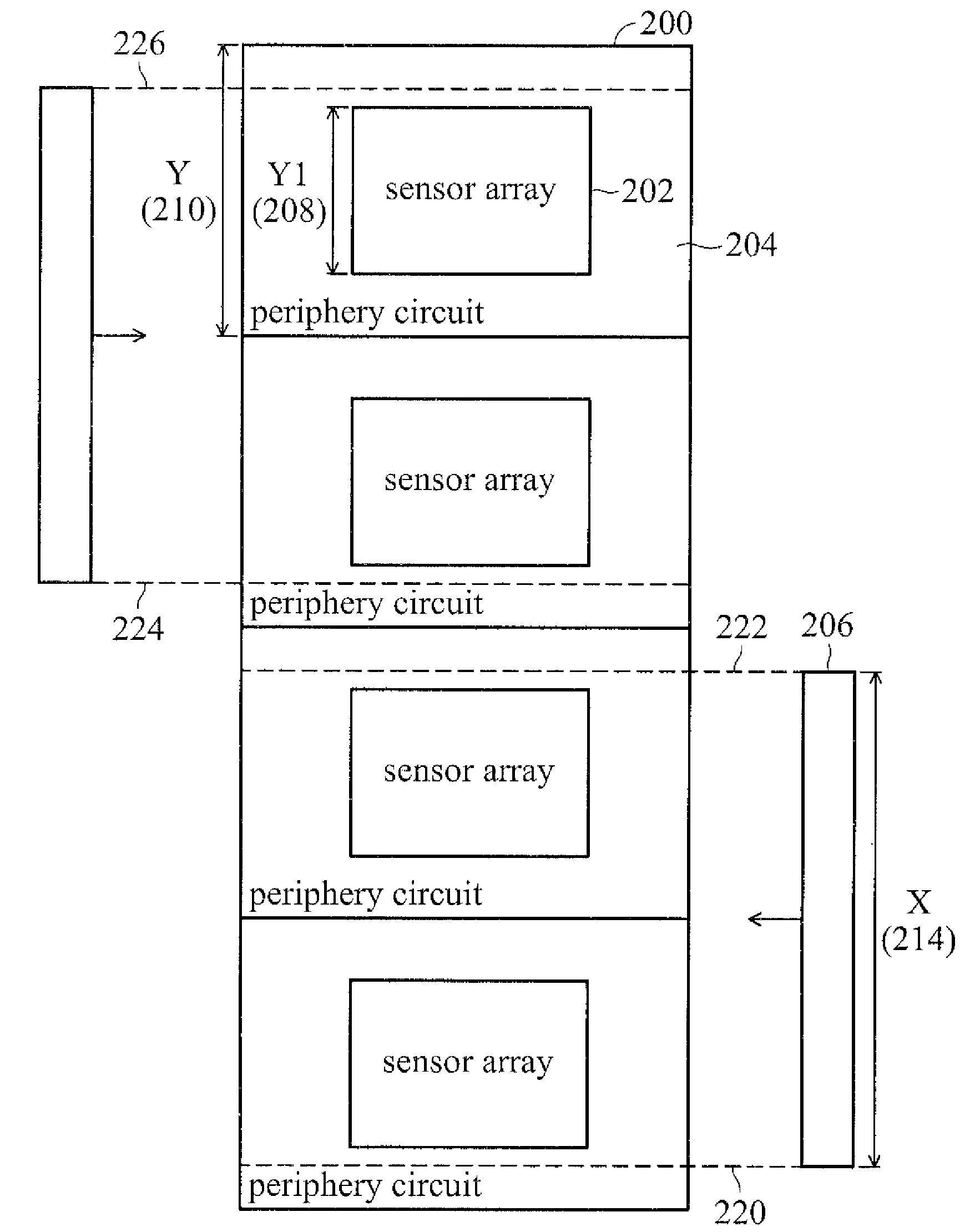
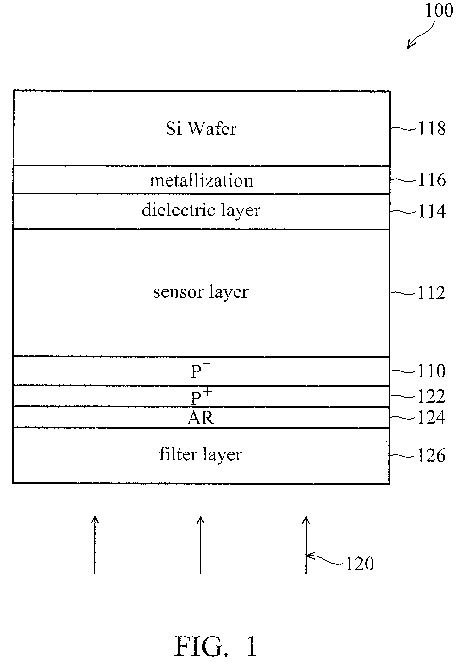
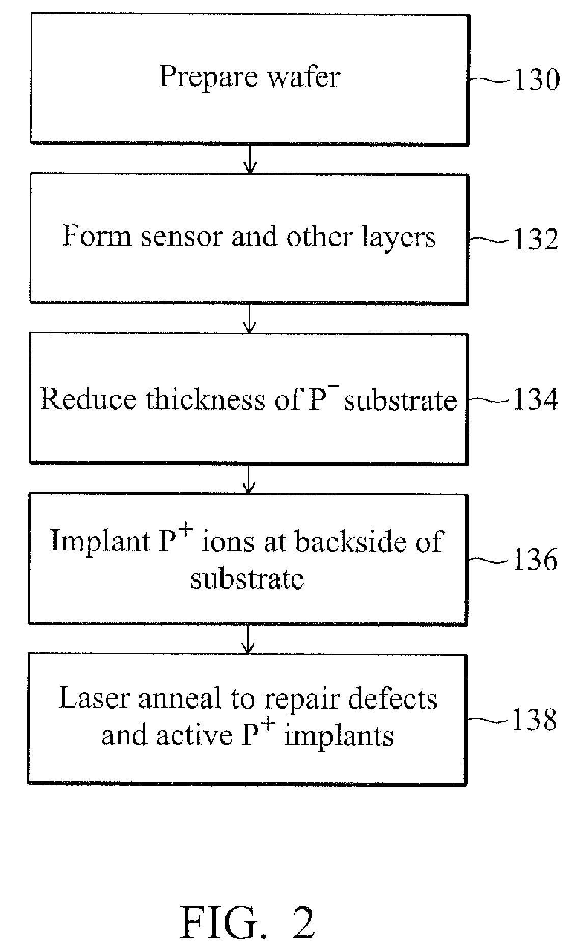
[0018]The present disclosure relates to methods for fabricating backside illumination (BSI) CMOS image sensor arrays to avoid dark-mode stripe pattern corresponding to laser scan boundary effects on the image sensor arrays during laser annealing. It is understood that the present disclosure provides many different foams and embodiments, and that specific embodiments are provided only as examples. Further, the scope of the present disclosure will only be defined by the appended claims. In the drawings, the sizes and relative sizes of layers and regions may be exaggerated for clarity. It will be understood that when an element or layer is referred to as being “on,”“connected to,” or “coupled to” another element or layer, it may be directly on, connected to, or coupled to the other element or layer, or intervening elements or layers may be present.

[0019]Spatially relative terms, such as “beneath,”“below,”“lower,”“above,”“upper” and the like, may be used herein for ease of description t...


PUM

PropertyMeasurementUnit
thicknessaaaaaaaaaa
thicknessaaaaaaaaaa
thicknessaaaaaaaaaa

Abstract

Methods are disclosed herein for determining the laser beam size and the scan pattern of laser annealing when fabricating backside illumination (BSI) CMOS image sensors to keep dark-mode stripe patterns corresponding to laser scan boundary effects from occurring within the sensor array regions of the image sensors. Each CMOS image sensor has a sensor array region and a periphery circuit. The methods determines a size of the laser beam from a length of the sensor array region and a length of the periphery circuit so that the laser beam covers an integer number of the sensor array region for at least one alignment of the laser beam on the array of BSI image sensors. The methods further determines a scan pattern so that the boundary of the laser beam does not overlap the sensor array regions during the laser annealing, but only overlaps the periphery circuits.

Description

TECHNICAL FIELD[0001]The present disclosure relates generally to methods for fabricating image sensors. Specifically, the present disclosure relates to methods for fabricating backside illumination (BSI) CMOS image sensor arrays.BACKGROUND[0002]An image sensor consists of an array of light sensitive picture elements (pixels) arranged in a sensor array region and periphery circuit elements. The pixels of the sensor array region respond to light incident on the pixels from a subject scene by generating electrical charges. The periphery circuit elements receive and process the generated electrical charges to display an image of the subject scene.[0003]Image sensors may be fabricated on a semiconductor substrate using complementary metal-oxide-semiconductor (CMOS) circuits and fabrication techniques. In CMOS image sensors, each pixel consists of a photodiode formed on a semiconductor substrate and additional layers formed on the photodiode. These additional layers include one or more di...

Claims


Application Information

Patent Timeline
Patent Type & Authority Patents(United States)
IPC IPC(8): H01L21/31
CPCH01L21/268H01L27/1464H01L27/14698H01L27/14643
Inventor HSU, KAI-CHUNTU, YEUR-LUENWANG, CHUNG CHIENHSU, TZU-HSUANWANG, CHING-CHUN
Owner TAIWAN SEMICON MFG CO LTD
Learn More