Power supply circuit and display device including the same

a technology of power supply circuit and display device, which is applied in the direction of electric variable regulation, process and machine control, instruments, etc., can solve the problems of difficult implementation of converters as semiconductor circuits, size reduction, etc., and achieve the effect of eliminating voltage drop, simple configuration, and reducing cos

Inactive Publication Date: 2012-11-20
SHARP KK
View PDF17 Cites 3 Cited by
  • Summary
  • Abstract
  • Description
  • Claims
  • Application Information

AI Technical Summary

Benefits of technology

[0071]According to the second aspect of the present invention, when generating the voltage which is to be supplied to the control terminal of the output-side switching element in order to turn ON the output-side switching element, the boosted voltage is supplied from the main boosting capacitor to the control-boosting capacitor via a control-boosting switching element. In this process, the control terminal of the control-boosting switching element is supplied with a voltage which is higher than the boosted voltage by at least the threshold voltage of the control-boosting switching element. This eliminates voltage drop by threshold value in the control-boosting switching element, and it is now possible to reliably generate a voltage which is higher than the boosted voltage by at least the threshold voltage of the output-side switching element as a voltage that is to be supplied to the control terminal of the output-side switching element when turning ON the output-side switching element. The arrangement more reliably removes influences of voltage drop by threshold value on the boosted supply voltage which is outputted from the power supply circuit.
[0072]According to the third aspect of the present invention, two clock signals each having the same amplitude as the other and a voltage alternating oppositely to each other are supplied as the first and the second clock signals to the first and the second input terminals respectively. Along with this, the third input terminal is supplied with the third clock signal which has a voltage alternating between predetermined low and high levels with an amplitude greater than the threshold voltage of the output-side switching element, and is maintained at the high level during its period except for a predetermined time near a time point at which there is a voltage change in the first and the second clock signals. In this arrangement, charging and boosting take place in the first capacitor and the second capacitor alternately and complementary to each other. Specifically, in one operation state a boosted voltage obtained at the first terminal of the first capacitor is outputted via the first switching element; in another operation state a boosted voltage obtained at the first terminal of the second capacitor is outputted via the second switching element; and these two operation states are repeated alternately to each other. While one of the first and the second capacitors is employed in boosting operation, the other is being charged. Such a complementary boosting cycle makes it possible to improve electric current supply capability to a load.
[0073]Also according to the third aspect of the present invention, when turning ON the first switching element which serves as the output-side switching element, a boosted voltage obtained at the first terminal of the first capacitor is supplied to the third capacitor and is boosted further by the third clock signal, whereby a voltage which is higher than the originally boosted voltage by at least the threshold voltage of the first switching element is supplied to the control terminal of the first switching element. Likewise, when turning ON the second switching element which serves as the output-side switching element, a boosted voltage obtained at the first terminal of the second capacitor is supplied to the fourth capacitor and is boosted further by the third clock signal, whereby a voltage which is higher than the originally boosted voltage by at least the threshold voltage of the second switching element is supplied to the control terminal of the second switching element. The arrangement ensures that the boosted voltages obtained at the respective first terminals of the first and the second capacitors are outputted as the boosted supply voltage without voltage drop by threshold value in the first and the second switching elements. Therefore, it is possible to output a desired boosted supply voltage reliably without being affected by the threshold voltage of the N-channel transistors or variation thereof even in cases where all of the switching elements in both of the booster section and the booster control section are provided by N-channel transistors.
[0074]According to the fourth aspect of the present invention, the third capacitor, which has its first terminal connected with the control terminal of the first switching element serving as the output-side switching element, is connected at its first terminal with the power supply terminal via the seventh switching element. This arrangement ensures that even in a case where the fifth switching element happens to have an unexpectedly large variation in its threshold value so as to be unable to turn ON the first switching element, it is still possible to turn ON the first switching element by boosting a voltage which is supplied to the third capacitor via the seventh switching element. Likewise, the fourth capacitor, which has its first terminal connected with the control terminal of the second switching element serving as the output-side switching element, is connected at its first terminal with the power supply terminal via the eighth switching element. This arrangement ensures that even in a case where the sixth switching element happens to have an unexpectedly large variation in its threshold value so as to be unable to turn ON the second switching element, it is still possible to turn ON the second switching element by boosting a voltage which is supplied to the fourth capacitor via the eighth switching element.
[0075]According to the fifth aspect of the present invention, when generating the voltage which is to be supplied to the control terminal of the output-side switching elements (the first and the second switching elements) in order to turn ON these switching elements, the boosted voltage is supplied from the main boosting capacitors (the first and the second capacitors) to the control-boosting capacitors (the third and the fourth capacitors) via the control-boosting switching elements (the fifth and the sixth switching elements). Meanwhile, the control terminal of the respective control-boosting switching elements (the fifth and the sixth switching elements) are supplied with a voltage which is higher than the said boosted voltage by at least the threshold voltage of the control-boosting switching elements. The arrangement makes it possible to reliably generate a voltage which is higher than the boosted voltage by at least the threshold voltage of the output-side switching element as a voltage that is to be supplied to the control terminal of the output-side switching element when turning ON the output-side switching element.
[0076]According to the sixth aspect of the present invention, a clock signal of a voltage which changes oppositely to the third clock signal and of an amplitude which is greater at least than a threshold voltage of the fifth and the sixth switching elements serving as the control-boosting switching element is supplied as the fourth clock signal to the fourth input terminal, whereby the control-boosting switching elements have their respective control terminals supplied with a voltage which is higher than the boosted voltage obtained at the first terminal of the main boosting capacitor by at least the threshold voltage of the control-boosting switching element. Specifically, during a steady operation, the boosted supply voltage is held in the first and the second internal control capacitors, and when generating the voltage which is to be supplied to the control terminals of the output-side switching elements in order to turn ON these switching elements, the boosted voltage is supplied from the main boosting capacitors to the control-boosting capacitors via the control-boosting switching elements. In this process, the boosted supply voltage which is obtained at the first terminal of the second internal control capacitor is boosted by the fourth clock signal. Thus, the control terminal of the control-boosting switching element is supplied with a voltage which is higher than the originally boosted voltage by at least the threshold voltage of the control-boosting switching elements. This eliminates voltage drop by threshold value in the control-boosting switching elements, ensuring reliable generation of a voltage which is higher than the boosted voltage by at least the threshold voltage of the output-side switching element as a voltage that is to be supplied to the control terminal of the output-side switching element when turning ON the output-side switching element.
[0077]According to the seventh aspect of the present invention, since there is no voltage drop by threshold value in the output-side switching element of the boosting section even if the switching elements are solely provided by N-channel transistors, it is possible to form a power supply circuit which is capable of outputting a desired boosted supply voltage reliably, on an insulated substrate such as a glass substrate, using N-channel transistors made of polycrystal silicon whose threshold value is higher and variation thereof is wider than those made of monocrystal silicon.
[0078]According to the eighth aspect of the present invention, since there is no voltage drop by threshold value in the output-side switching element of the boosting section even if the switching elements are solely provided by N-channel transistors, it is possible to form a power supply circuit which is capable of outputting a desired boosted supply voltage reliably, on an insulated substrate such as a glass substrate, using N-channel transistors provided by thin film transistors whose threshold value is higher and variation thereof is wider than those made of monocrystal silicon.
[0079]According to the ninth aspect of the present invention, a driver monolithic display device includes a substrate formed thereon with a voltage boosting power supply circuit together with a plurality of pixel circuits and at least part of a driving circuit. In this configuration, the power supply circuit uses N-channel transistors for all of its switching elements, and yet is capable of outputting a desired boosted supply voltage reliably without a voltage drop by threshold value. Thus, the present invention enables size reduction of display devices and cost reduction in the manufacture thereof.
[0080]According to the tenth aspect of the present invention, a driver monolithic display device includes a substrate formed thereon with a voltage boosting power supply circuit together with a plurality of pixel circuits and at least part of a driving circuit. In this configuration, the power supply circuit is capable of outputting a desired boosted supply voltage reliably without a voltage drop by threshold value. Further, switching elements constituting these pixel circuits, the part of driving circuit and the power supply circuit which are formed on the same substrate are solely provided by N-channel thin film transistors. This enables simultaneous formation and cost reduction thereby of these circuits, to be achieved through a fewer number of manufacturing steps than necessary for cases which require both N-channel thin film transistors and P-channel thin film transistors.

Problems solved by technology

A challenge with this type of DC-DC converters, however, is size reduction since the converter requires inductive elements, and it has long been difficult to implement the converter as a semiconductor circuit.

Method used


Image

  • Power supply circuit and display device including the same
  • Power supply circuit and display device including the same
  • Power supply circuit and display device including the same

Examples


Embodiment Construction

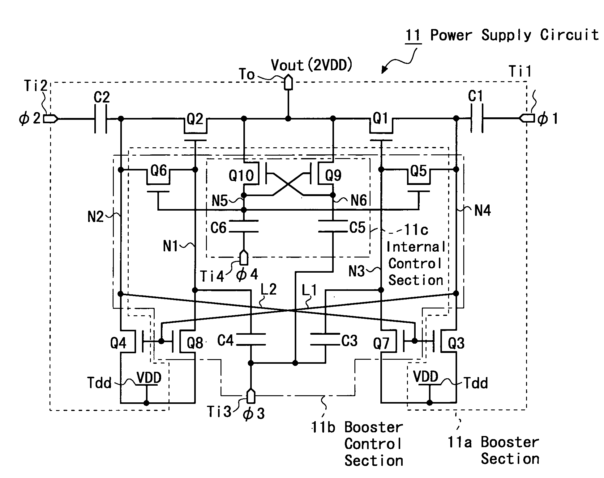
[0143]Hereinafter, an embodiment of the present invention will be described with reference to the attached drawings.

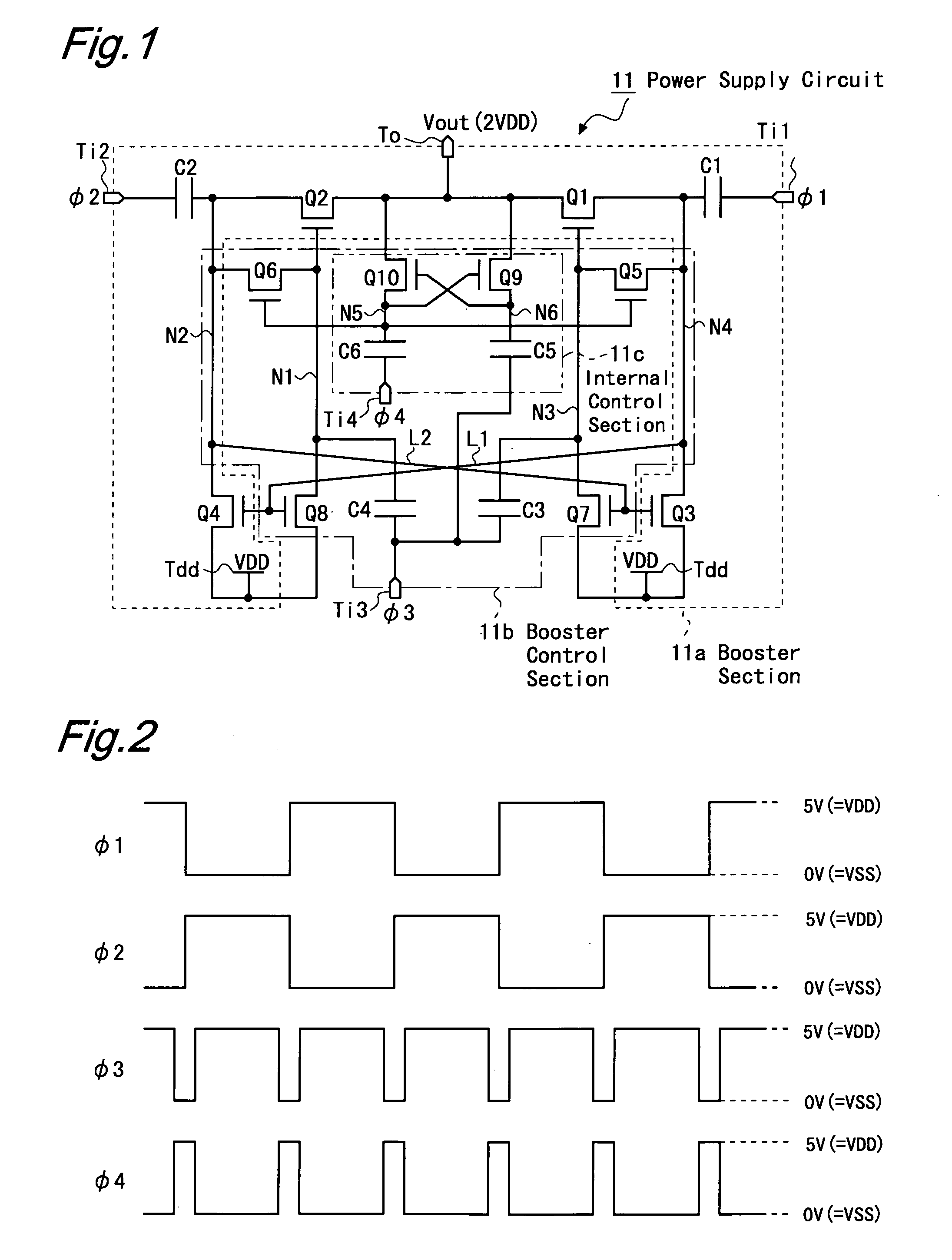
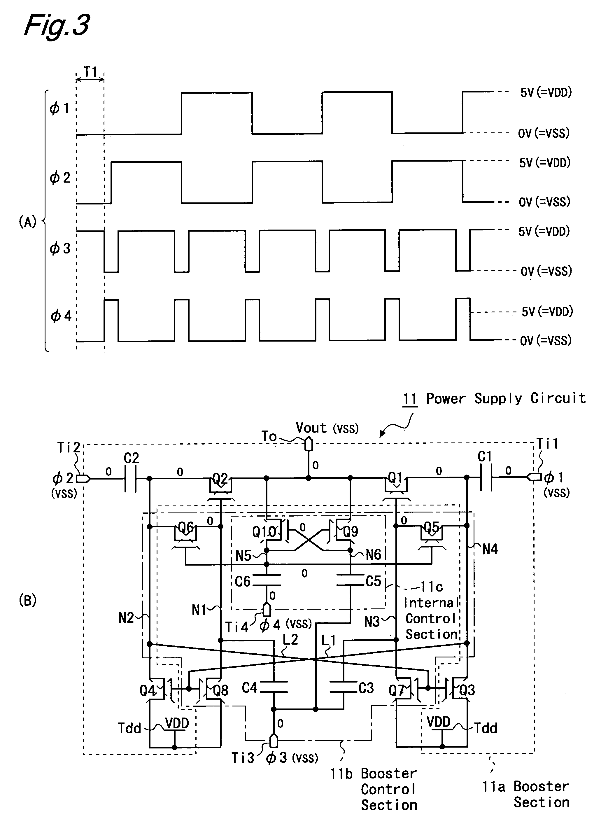
[0144]FIG. 1 is a circuit diagram which shows a configuration of a power supply circuit according to an embodiment of the present invention. This power supply circuit 11 includes: a booster section 11a which boosts an externally supplied input supply voltage VDD (>0) in a complimentary manner thereby generating a boosted supply voltage Vout (=2VDD); and a booster control section 11b which supplies the booster section 11a with signals for controlling the voltage boosting operation; and has external terminals including: a first and a second input terminals Ti1 and Ti2 for receiving externally supplied first and second clock signals φ1 and φ2 respectively; a third input terminals Ti3 for receiving a third clock signal φ3 for boosting the signals which controls the booster section 11a; a fourth input terminals Ti4 for receiving an externally supplied fourth clock signal φ4...


PUM


Abstract

An embodiment of the present invention provides a power supply circuit including a charge-pumping booster section which uses switching elements provided only by N-channel transistors yet does not have a problem of voltage drop by threshold value. When a boosted voltage is obtained at a first terminal of a first capacitor in a booster section, a booster control section supplies this boosted voltage to a third capacitor, to boost the voltage further thereby turning ON a first transistor. When a boosted voltage is obtained at a first terminal of a second capacitor in the booster section, the booster control section supplies this boosted voltage to a fourth capacitor, to boost the voltage further thereby turning ON a second transistor. This arrangement eliminates a problem of voltage drop by threshold value in the first and the second transistors which serve as output-side switching elements.

Description

TECHNICAL FIELD[0001]The present invention relates to power supply circuits, and more specifically to a power supply circuit which includes a charge-pumping booster section for boosting a supply voltage, and to a driver monolithic display device which includes such a power supply circuit.BACKGROUND ART[0002]Inductance DC-DC converters for boosting supply voltages are already public. A challenge with this type of DC-DC converters, however, is size reduction since the converter requires inductive elements, and it has long been difficult to implement the converter as a semiconductor circuit. For this reason, when supply voltage boosting is required in portable equipment such as mobile telephone terminals or in integrated circuits, the task is accomplished by charge pump circuits (see Patent Document 1 (JP-A H10-285911 Gazette), for example) which are built with capacitors and switching elements.[0003]In liquid crystal display devices incorporated in mobile telephone terminals for examp...

Claims


Application Information

Patent Timeline
Patent Type & Authority Patents(United States)
IPC IPC(8): G05F1/10
CPCH02M3/073H02M2003/077H02M3/077
Inventor NISHI, SHUJITSUJINO, SACHIOMURAKAMI, YUHICHIROHSASAKI, YASUSHIGYOUTEN, SEIJIROU
Owner SHARP KK
Why Eureka
Try Eureka