Organic diode display driving circuits, display panels and electronic devices

a driving circuit and diode technology, applied in the direction of electrical devices, semiconductor devices, instruments, etc., can solve the problems of different voltage drops caused by wirings, low driving voltage, and low power consumption, so as to eliminate the voltage drop reduce the resistance of power-supply wirings in the display area.

Inactive Publication Date: 2018-07-26
WUHAN CHINA STAR OPTOELECTRONICS TECH CO LTD
View PDF7 Cites 3 Cited by
  • Summary
  • Abstract
  • Description
  • Claims
  • Application Information

AI Technical Summary

Benefits of technology

[0026]By configuring the wirings in the auxiliary area to connect to the voltage line, the resistance of the power-supply wirings in the display area may be reduced so as to eliminate the voltage drop of the power-supply wirings in the display area.

Problems solved by technology

In particular, the driving voltage is low and the power consumption is low.
However, as the distances between each of the pixels within the AA pixel area and the pixel source are different, which results in that the voltage drops caused by the wirings are different.
Thus, the display uniformity of the panel may be affected.

Method used


Image

  • Organic diode display driving circuits, display panels and electronic devices
  • Organic diode display driving circuits, display panels and electronic devices
  • Organic diode display driving circuits, display panels and electronic devices

Examples


first embodiment

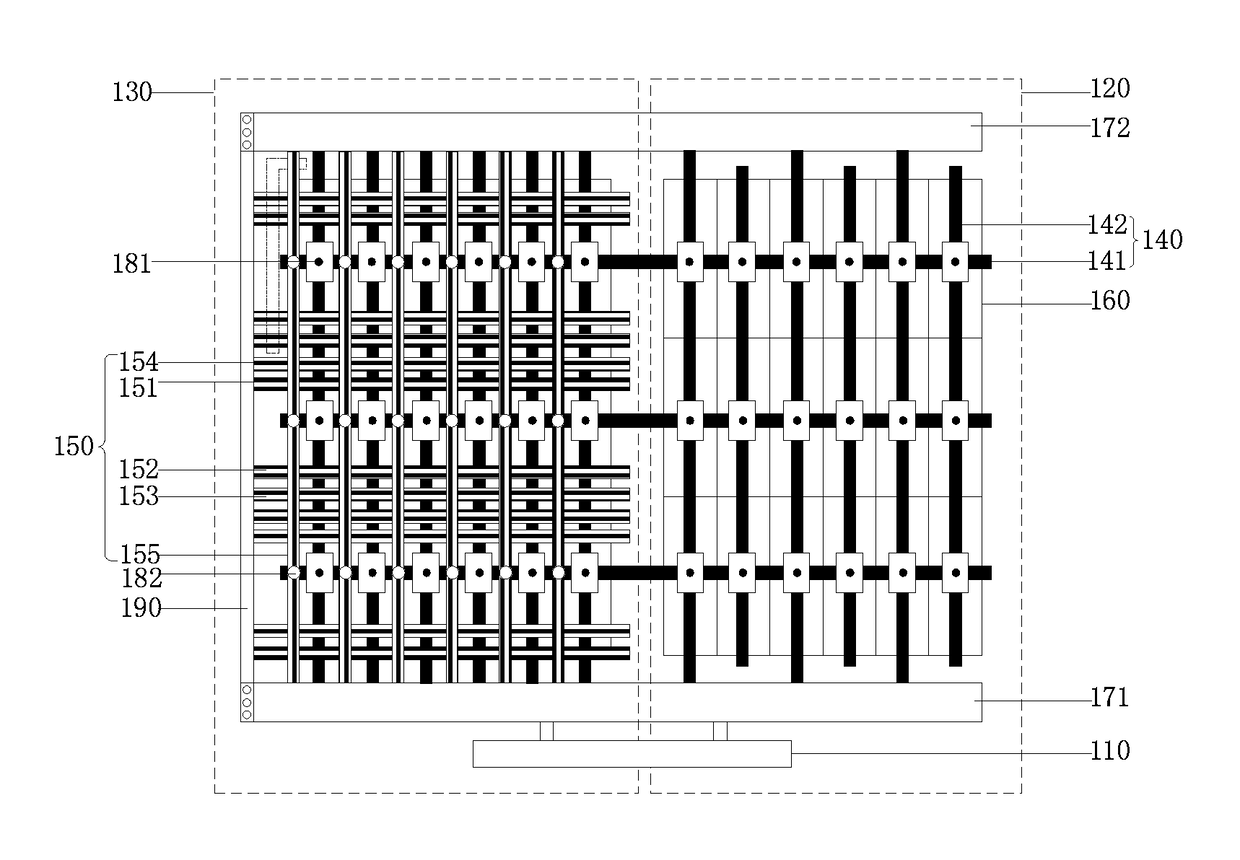
[0034]FIG. 1 is a schematic view of the organic diode display driving circuit in accordance with a The organic diode display driving circuit includes a voltage source 110, a display-area circuit 120, and an auxiliary-area circuit 130 arranged outside a display area. The voltage source 110 provides the voltage to the whole chip, the display-area circuit 120 and the auxiliary-area circuit 130 include power-supply wirings 140, signal wirings 150, and at least one pixel 160. The voltage source 110 connects to the pixel 160 within the display area via the power-supply wirings 140. The voltage source 110 further directly or indirectly connects to the pixel 160 within the display area via the signal wirings 150 in the auxiliary area.

[0035]Specifically, the signal wirings 150 in the auxiliary area includes one of or a combination including some of the first scanning line 151, a second scanning line 152, an initial-voltage line 153, a light-emitting control line 154 and a data line 155.

[003...

second embodiment

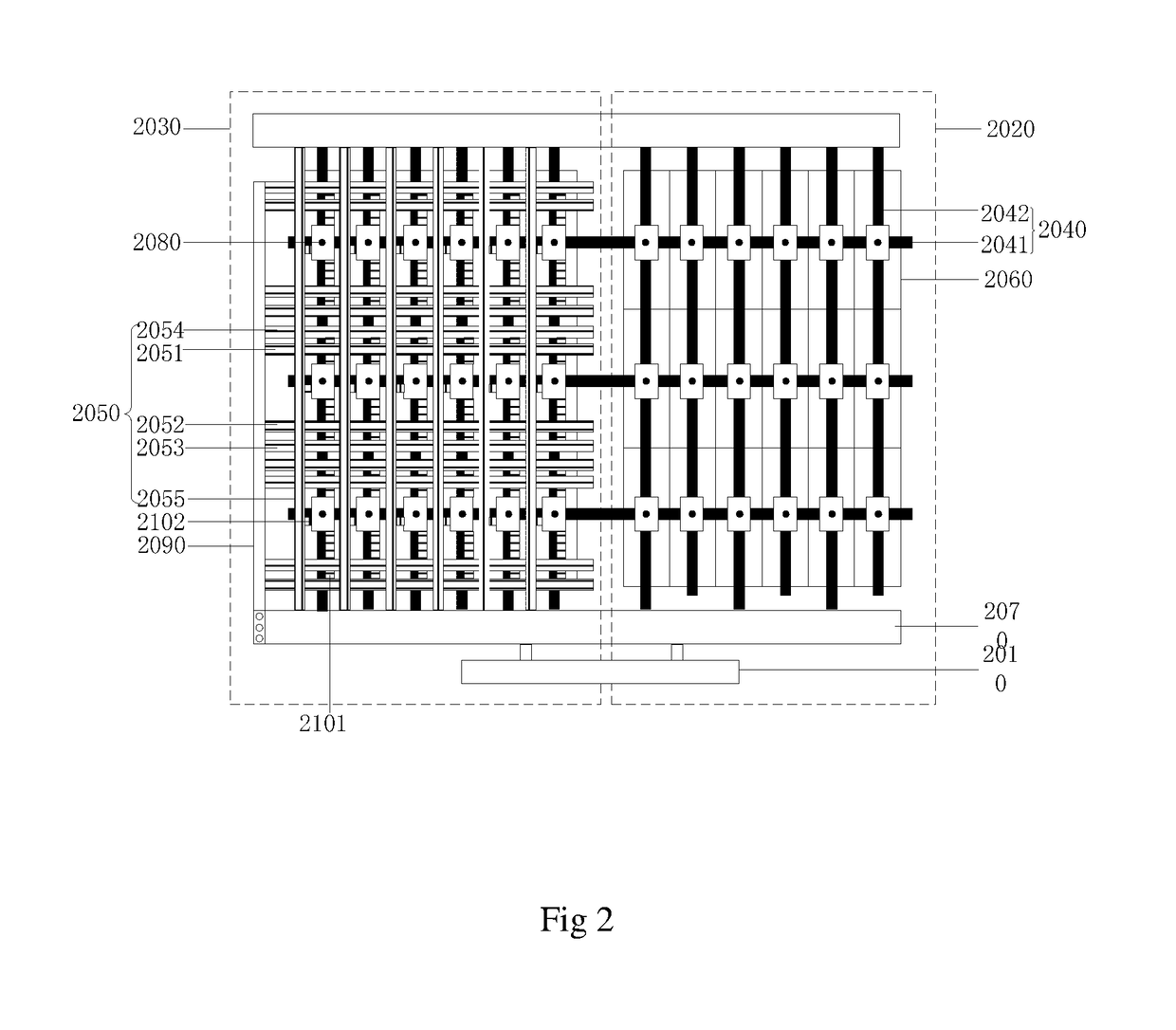
[0042]FIGS. 2 and 3 are directed to the organic diode display driving circuit in accordance with a The organic diode display driving circuit includes a voltage source 2010, a display-area circuit 2020, and an auxiliary-are circuit 2030, and the auxiliary area is outside of the display area. The display-area circuit 2020 and the auxiliary-are circuit 2030 both include power-supply wirings 2040, signal wirings 2050, and a pixel 2060. The voltage source 2010 connects to the pixel 2060 within the display area. The voltage source 2010 further directly or indirectly connects to the pixel 2060 within the display area via the signal wirings 2050 in the auxiliary area.

[0043]The signal wirings 2050 include one of or a combination of some of the first scanning line 2051, a second scanning line 2052, an initial voltage line 2053, a light-emitting control ling 2054 and the data line 2055.

[0044]The power-supply wirings 2040 include row power-supply lines 2041 and column power-supply lines 2042 a...


PUM


Abstract

The present disclosure relates to an organic diode display driving circuit, a display panel, and an electronic device. The driving circuit includes a voltage source, a display-area circuit, and an auxiliary-area circuit being arranged outside a display area. The display-area circuit and the auxiliary-area circuit include power-supply wirings, signal wirings, and at least one pixel, and the voltage source connects to the pixel within the display area via the power-supply wirings. The voltage source further directly or indirectly connects to the pixel within the display area via the wirings in an auxiliary area. By configuring the wirings in the auxiliary area to connect to the voltage line, the resistance of the power-supply wirings in the display area may be reduced so as to eliminate the voltage drop of the power-supply wirings in the display area.

Description

BACKGROUND OF THE INVENTION1. Field of the Invention[0001]The present disclosure relates to liquid crystal display technology, and more particularly to an organic diode display driving circuit, a display panel, and an electronic device.2. Discussion of the Related Art[0002]Active matrix organic light-emitting diode (OLED) panels generally includes very thin organic coating layers and a glass substrate. When the current passes by, the organic material emits light. The OLED panels are characterized by self-light-emitting, wide viewing angle, and high saturation. In particular, the driving voltage is low and the power consumption is low. In addition, the OLED panels also have the advantages such as quick response time, light weight, thin thickness, simple structure, and low lost, and thus have been deemed as the most potential product.[0003]OLED panels include a normal pixel area (AA pixel area) and a virtual pixel area. The virtual pixel area is designed to alleviate the loading effec...

Claims


Application Information

Patent Timeline
Patent Type & Authority Applications(United States)
IPC IPC(8): G09G3/3258H01L27/32H01L51/56
CPCG09G3/3258H01L27/3276H01L51/56G09G2300/0809G09G2300/02G09G3/3233G09G2300/0426G09G2300/0819G09G2300/0861G09G2310/0251G09G2320/0223H10K59/131H10K71/00
Inventor YI, SHIJUAN
Owner WUHAN CHINA STAR OPTOELECTRONICS TECH CO LTD
Why Eureka
Try Eureka