
Voltage amplifier and driving device of display device using the voltage amplifier

a technology of voltage amplifier and driving device, which is applied in the direction of logic circuit coupling/interface arrangement, static indicating device, instruments, etc., can solve the problem of increasing power consumption

Inactive Publication Date: 2012-11-20
MC TECH CO LTD
View PDF14 Cites 83 Cited by
  • Summary
  • Abstract
  • Description
  • Claims
  • Application Information

AI Technical Summary

Benefits of technology

"The present invention provides an amplifying circuit for a liquid crystal display (LCD) that reduces the number of input transistors and the driving device of the display device using the same. The amplifying circuit includes an input unit, a bias unit, and an output unit. The input unit receives a first input signal and the bias unit applies bias voltages to the transistors. The output unit includes transistors and capacitors to transmit the output voltage. The technical effect of this invention is to reduce the area occupied by the input transistor and power consumption while maintaining the same electrical characteristics."

Problems solved by technology

Accordingly, the conventional amplifying circuit has a problem of increasing the area occupied by the input transistor from among the entire area of the amplifying circuit because of adopting the rail-to-rail structure, and generates a problem of increasing power consumption because constant current sources for the input transistors of different types must be used.

Method used


Image

  • Voltage amplifier and driving device of display device using the voltage amplifier
  • Voltage amplifier and driving device of display device using the voltage amplifier
  • Voltage amplifier and driving device of display device using the voltage amplifier

Examples


Embodiment Construction

Technical Problem

[0017]The present invention has been made in an effort to provide an amplifying circuit for reducing a number of input transistors and a driving device of a display device using the same.

Technical Solution

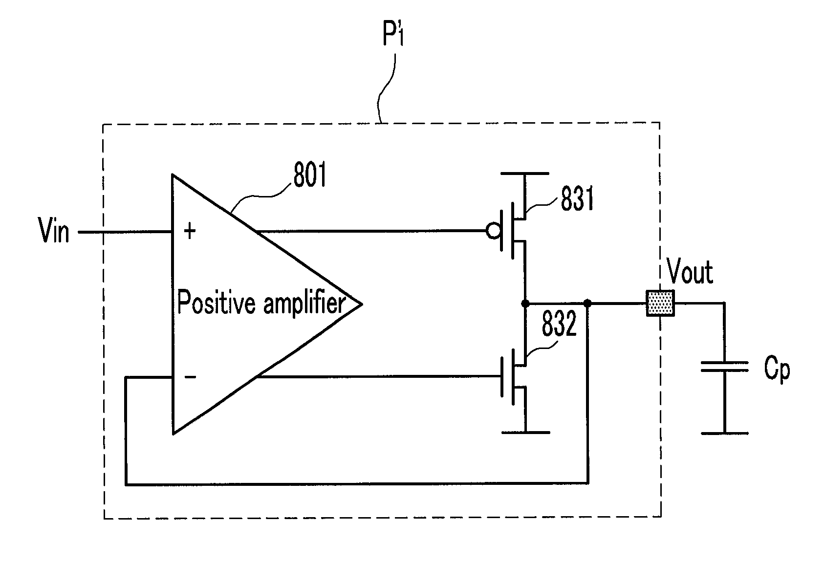
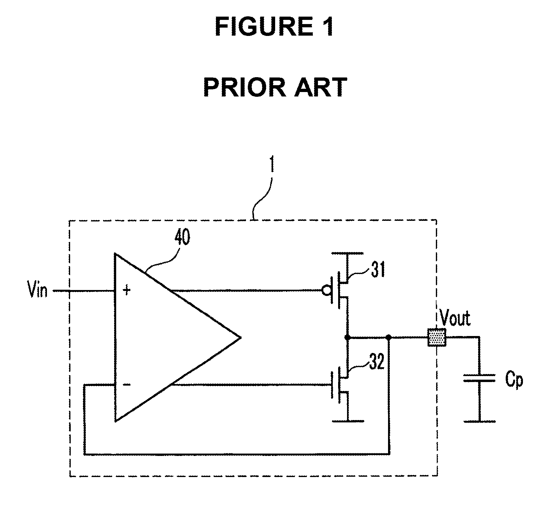
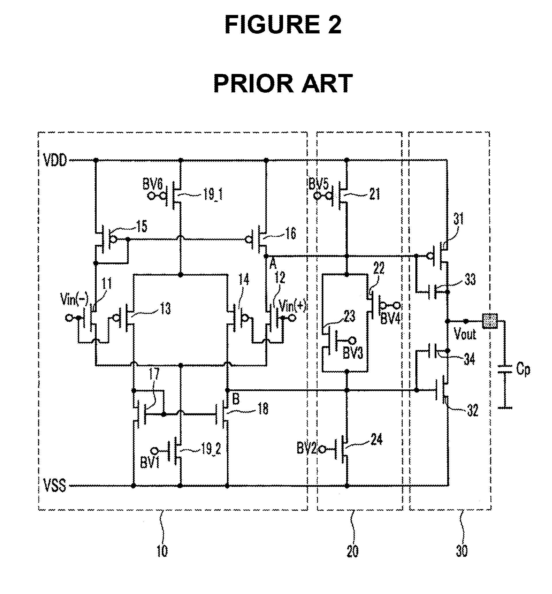
[0018]An exemplary embodiment of the present invention provides an amplifying circuit for a liquid crystal display (LCD) including a plurality of pixels, including: an input unit, coupled between a first power source for supplying a first voltage and a second power source for supplying a second voltage, for receiving a first input signal and a second input signal, and being controllable by the first and second input signals; a bias unit for receiving a bias voltage for operating the input unit, and including a first node and a second node controlled by the input unit; and an output unit for applying an output voltage to the pixel by using a first output transistor being turned on / off according to a signal applied to the first node and a second output transistor bei...


PUM


Abstract

An amplifying circuit of a display device including a plurality of pixels includes an input unit, a bias unit, and an output unit. The input unit is coupled between a first power source for supplying a first voltage and a second power source for supplying a second voltage, receives a first input signal and a second input signal, and is controlled by the first and second input signals. The bias unit receives a bias voltage for operating the input unit, and includes a first node and a second node controllable by the input unit. The output unit applies an output voltage to a pixel by using a first output transistor turned on / off by a signal applied to the first node and a second output transistor turned on / off by a signal applied to the second node, and the first output transistor is a different type to the second output transistor. In this instance, the input unit includes a first input transistor having a first terminal coupled to a first power source and being turned on / off by a first input signal and a second input transistor of the same type as the first input transistor, having a first terminal coupled to the first power source, and being turned on / off by a second input signal. The bias unit includes a first transistor controllable by the on / off state of the first input transistor and a second transistor controllable by the on / off state of the second input transistor.

Description

TECHNICAL FIELD[0001]The present invention relates to an amplifying circuit and a driving device of a display device using the same. More particularly, the present invention relates to an amplifying circuit having less power consumption, a reduced area, and the same electrical characteristics as a conventional circuit.BACKGROUND ART[0002]Recently, as personal computers and televisions have been become lighter and slimmer, display devices have also been required to become lighter and slimmer, and flat displays such as liquid crystal displays (LCD) other than cathode ray tubes (CRT) have been increasingly researched according to the requirements.[0003]The liquid crystal display (LCD) is a display device for acquiring a desired video signal by applying an electric field to a liquid crystal material having an anisotropic dielectric constant and injected between two substrates, controlling an intensity of the electric field, and controlling the light transmitted to the substrates from an...

Claims


Application Information

Patent Timeline
Patent Type & Authority Patents(United States)
IPC IPC(8): G09G3/36
CPCG09G3/3688H03F1/34H03F3/3022H03F3/45183H03F3/45192H03F3/45475G09G2330/021H03F2200/297H03F2203/30021H03F2203/45028H03F2203/45632G09G3/36H03K19/0175H03F3/45G02F1/133
Inventor KIMPARK, HEE-JONGNO, JU-YOUNGLEE, SANG-HOON
Owner MC TECH CO LTD
Learn More