Semiconductor device

a semiconductor chip and semiconductor technology, applied in the direction of pulse technique, electronic switching, emergency protective circuit arrangement, etc., can solve the problems of solder cracks, solder fatigue, danger of etc., to prevent thermal failure of semiconductor chips, enhance detection accuracy, and prevent solder cracks

Active Publication Date: 2012-12-04
FUJI ELECTRIC CO LTD
View PDF16 Cites 4 Cited by
  • Summary
  • Abstract
  • Description
  • Claims
  • Application Information

AI Technical Summary

Benefits of technology

[0016]In the above described device, the thermal resistance in the heat dissipation path from the semiconductor chip can be calculated, while actually operating the switching element. As a result it is possible to detect degradation of heat dissipation from the semiconductor chip even when the operating state of the semiconductor device cannot be predicted, and the occurrence of solder cracks can be ascertained reliably, so that thermal failure of the semiconductor chip can be prevented in advance.
[0018]Further, the thermal resistance calculation circuit preferably calculates the integrated value of losses occurring in the switching element and the temperature difference of the semiconductor chip based on the time elapsed until saturation of temperature in the heat dissipation path from the semiconductor chip and the semiconductor chip temperature difference, and calculates the thermal resistance at a specific location on the heat dissipation path from the semiconductor chip. By changing the interval of sampling of the semiconductor chip temperature, the thermal resistance at a specific location in the heat dissipation path from the semiconductor chip can be calculated, and even in cases in which heat dissipation mean are provided to dissipate heat generated from the semiconductor chip, anomalies in the solder layer can be detected, so that the occurrence of solder cracks can be ascertained accurately.
[0019]Further, the semiconductor is preferably characterized in that by setting the time interval, over which the integrated value of losses occurring in the switching element and the semiconductor chip temperature difference are calculated, to 200 ms or less, the thermal resistance calculation circuit monitors anomalies in the solder layer fixing the semiconductor chip to the mounting substrate, and by setting the time interval, over which the integrated value of losses occurring in the switching element and the semiconductor chip temperature difference are calculated, to two seconds or less, the thermal resistance calculation circuit monitors anomalies in the contact face of the heat dissipation means, and by setting the time interval, over which the integrated value of losses occurring in the switching element and the semiconductor chip temperature difference are calculated, to two seconds or more, the thermal resistance calculation circuit monitors anomalies in the heat dissipation means. By changing the time interval for sampling the semiconductor chip temperature, it is possible to monitor not only anomalies in the solder layer, but anomalies in the contact face of the heat dissipation means and anomalies in the heat dissipation means also, and the accuracy of detection of degradation of heat dissipation from the semiconductor chip can be enhanced.
[0020]Further, the semiconductor device is preferably characterized in further including a comparison mechanism that compares the thermal resistance calculated by the thermal resistance calculation circuit with a prescribed value, and a protection circuit which, when the thermal resistance calculated by the thermal resistance calculation circuit exceeds the prescribed value, either halts operation of the switching element, or limits the current flowing in the switching element. When a solder crack occurs, operation of the switching element can be halted, and thermal failure of the semiconductor chip can be prevented in advance.
[0021]Further, the semiconductor device preferably includes a control circuit that controls switching operation of the switching element; a thermal resistance prediction circuit that calculates the switching element loss and the temperature based on control information controlling switching operation, and predicts the thermal resistance in the heat dissipation path from the semiconductor chip; a comparison mechanism that compares the thermal resistance calculated by the thermal resistance calculation circuit with the thermal resistance predicted by the thermal resistance prediction circuit; and a protection circuit which, when the thermal resistance calculated by the thermal resistance calculation circuit exceeds the thermal resistance predicted by the thermal resistance prediction circuit, either halts operation of the switching element, or limits the current flowing in the switching element. In such a device, while taking into consideration the thermal resistance of the unit as a whole, operation of the switching element can be halted, and thermal failure of the semiconductor chip can be prevented in advance.
[0022]As explained above, by means of this invention the thermal resistance in the heat dissipation path from the semiconductor chip can be calculated while actually operating a switching element. Hence even when the operating state of the semiconductor device cannot be predicted, degradation of heat dissipation from the semiconductor chip can be detected, and the occurrence of solder cracks can be reliably ascertained, so that thermal failure of the semiconductor chip can be prevented in advance.

Problems solved by technology

These members have large differences in thermal expansion coefficient, and stresses and strains occur between these members due to temperature cycles, so that the solder undergoes fatigue, and solder cracks occur.
When a solder crack occurs, heat dissipation from the semiconductor chip is degraded, and the temperature of the semiconductor chip rises rapidly, leading to the danger of thermal failure of the semiconductor chip.
However, in methods to predict the lifetime of a semiconductor element, there is the problem that, if the model case used in lifetime prediction differs from the actual operation pattern during operation, lifetime prediction may not be possible, or it may not be possible to avoid the danger that thermal failure of the semiconductor chip.
Further, in methods to monitor the temperature of the semiconductor chip, there is the problem that, when the semiconductor device operates at or below the rated current, even when a solder crack occurs, an anomalous increase in temperature of the semiconductor chip cannot be detected, and thermal failure of the semiconductor chip cannot be prevented in advance.

Method used


Image

  • Semiconductor device
  • Semiconductor device
  • Semiconductor device

Examples


Embodiment Construction

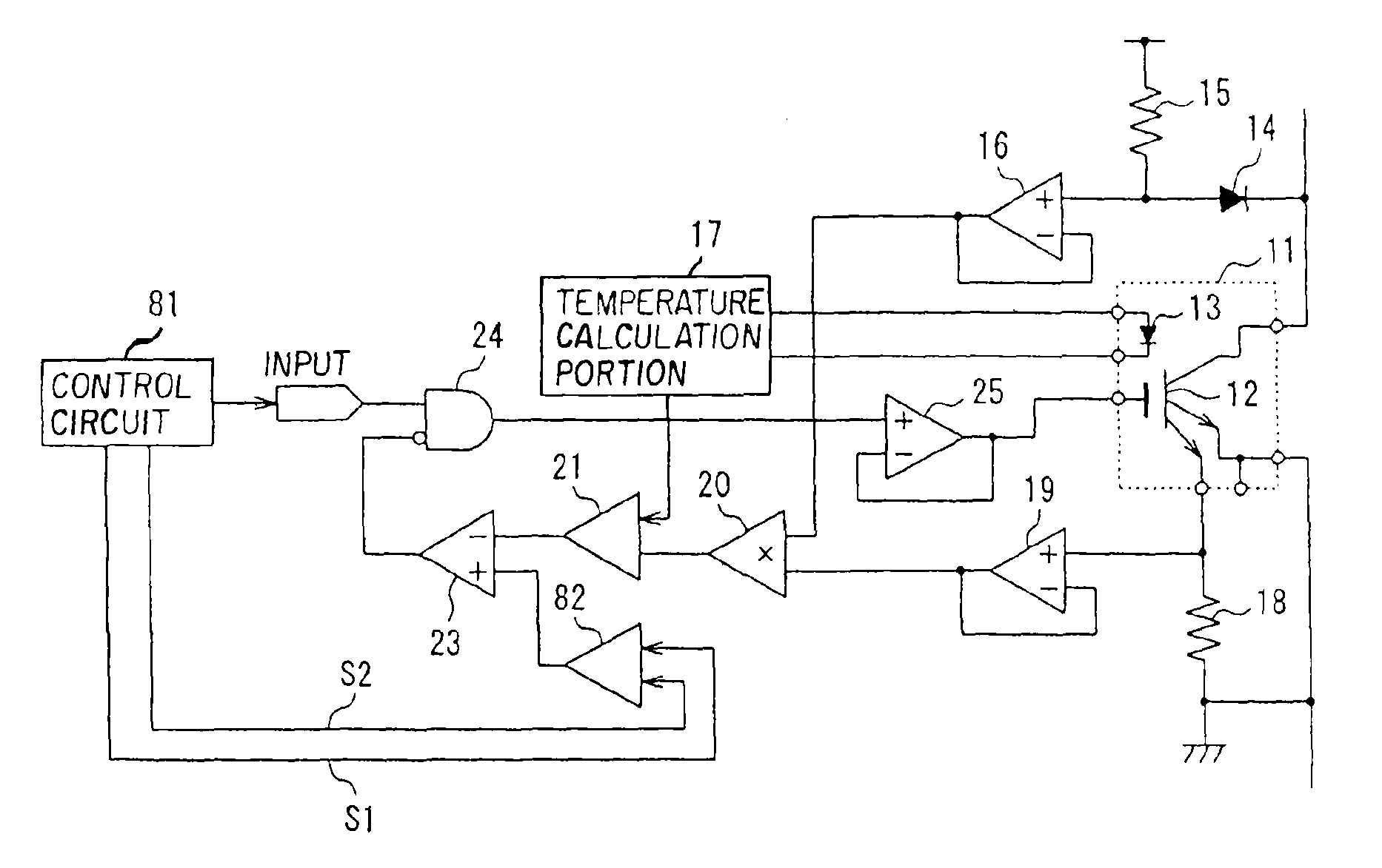
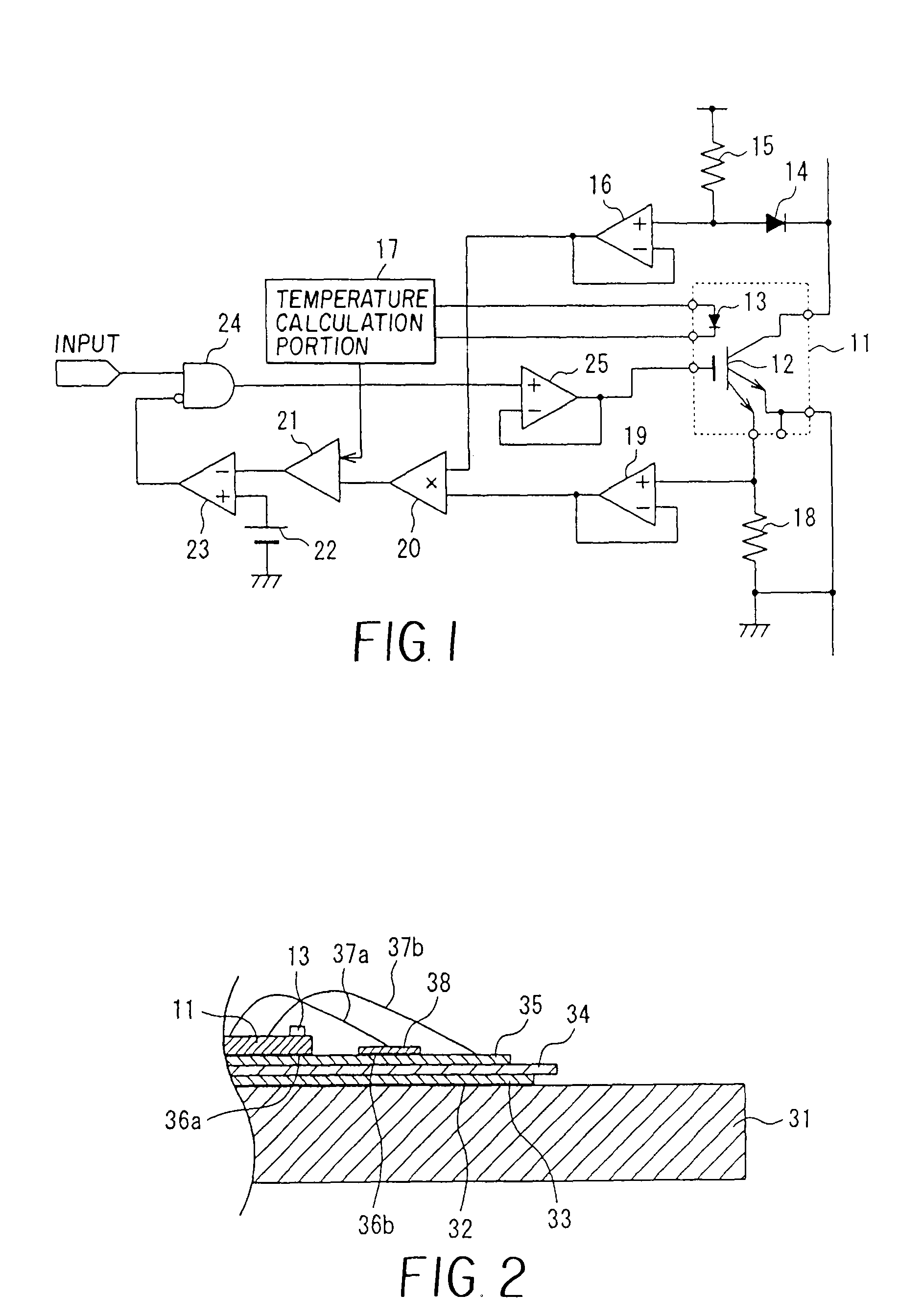
[0031]Semiconductor devices in accordance with the invention will now be explained in greater detail. FIG. 1 is a block diagram showing in summary the configuration of the semiconductor device of a first aspect of the invention. In FIG. 1, a switching element 12 which performs switching operation and a diode 13 used to detect the temperature of the semiconductor chip 11 are formed on the semiconductor chip 11. As the switching element 12, an IGBT (Insulated Gate Bipolar Transistor), a bipolar transistor, or a power MOSFET can be used. The semiconductor chip 11 can be mounted on a copper base with high thermal conductivity, with a ceramic substrate interposed for insulation, and solder can be used for bonding of members between the semiconductor chip and the copper base.

[0032]The semiconductor device provided with the semiconductor chip 11 is also provided with a voltage detection circuit 16 that detects the voltage applied to the switching element 12; a current detection circuit 19 ...


PUM


Abstract

In order to enable detection of degradation of the heat dissipation from a semiconductor chip, even when the operating state of a semiconductor device cannot be predicted, a thermal resistance calculation circuit calculates the thermal resistance of the heat dissipation path from the semiconductor chip, based on the loss of a switching element calculated by a loss calculation circuit and the temperature of the semiconductor chip calculated by a temperature calculation portion, and when the voltage corresponding to the thermal resistance calculated by the thermal resistance calculation circuit exceeds a reference voltage, switching operation of the switching element is halted.

Description

BACKGROUND[0001]The invention relates in general to a semiconductor device, and in particular relates to a semiconductor device which is suitable for application as a device provided with functions to monitor thermal resistance.[0002]In power semiconductor devices, a semiconductor chip is mounted on a copper base with high thermal conductivity so as to efficiently dissipate heat from the semiconductor chip, with a ceramic substrate for insulation interposed, and solder is used for bonding of members between the semiconductor chip and the copper base. These members have large differences in thermal expansion coefficient, and stresses and strains occur between these members due to temperature cycles, so that the solder undergoes fatigue, and solder cracks occur. When a solder crack occurs, heat dissipation from the semiconductor chip is degraded, and the temperature of the semiconductor chip rises rapidly, leading to the danger of thermal failure of the semiconductor chip.[0003]In ord...

Claims


Application Information

Patent Timeline
Patent Type & Authority Patents(United States)
IPC IPC(8): H02H5/04
CPCH03K17/0822H03K2017/0806H01L2924/0002H01L2924/00
Inventor ICHIKAWA, HIROAKI
Owner FUJI ELECTRIC CO LTD
Why Eureka
Try Eureka