
A/D conversion circuit, solid-state image sensor, and camera system

a conversion circuit and image sensor technology, applied in the field of a/d conversion circuits, solid-state image sensors, camera systems, etc., can solve the problems of increasing the operation electrical current of the operation, increasing noise, and complex systems, and achieving the effect of difficult distortion of the duty of counting operations

Active Publication Date: 2012-12-11
SONY CORP
View PDF17 Cites 21 Cited by
  • Summary
  • Abstract
  • Description
  • Claims
  • Application Information

AI Technical Summary

Benefits of technology

The present invention relates to an A / D conversion circuit that includes a comparator and a counter. The comparator compares a signal potential with a reference voltage and outputs a determination signal regarding the comparison. The counter controls the operation of the comparator and performs additional functions such as switching between up and down counts, performing counting at both rising and falling edges of an input clock, and latching the input clock. The technical effect of this invention is to improve the accuracy and efficiency of A / D conversion circuits in image sensors and camera systems.

Problems solved by technology

The reason for this is that various problems including the system becoming very complex because dedicated processes are necessary in the manufacture of CCD pixels, a plurality of power-supply voltages being necessary for the operations thereof, and furthermore, a plurality of peripheral ICs needing to be combined and operated, are overcome by using CMOS image sensors.
Therefore, noise is not generated in this sampling process, but noise is carried when the voltage level of the preceding capacitor is reset to a certain reference value.
However, in the above-described method, a counter circuit exists in each column, and many counters perform counting operations at the time of A / D conversion, thereby presenting a problem in that the operation electrical current thereof is increased.

Method used


Image

  • A/D conversion circuit, solid-state image sensor, and camera system
  • A/D conversion circuit, solid-state image sensor, and camera system
  • A/D conversion circuit, solid-state image sensor, and camera system

Examples


Embodiment Construction

[0042]Embodiments of the present invention will be described below in conjunction with the drawings.

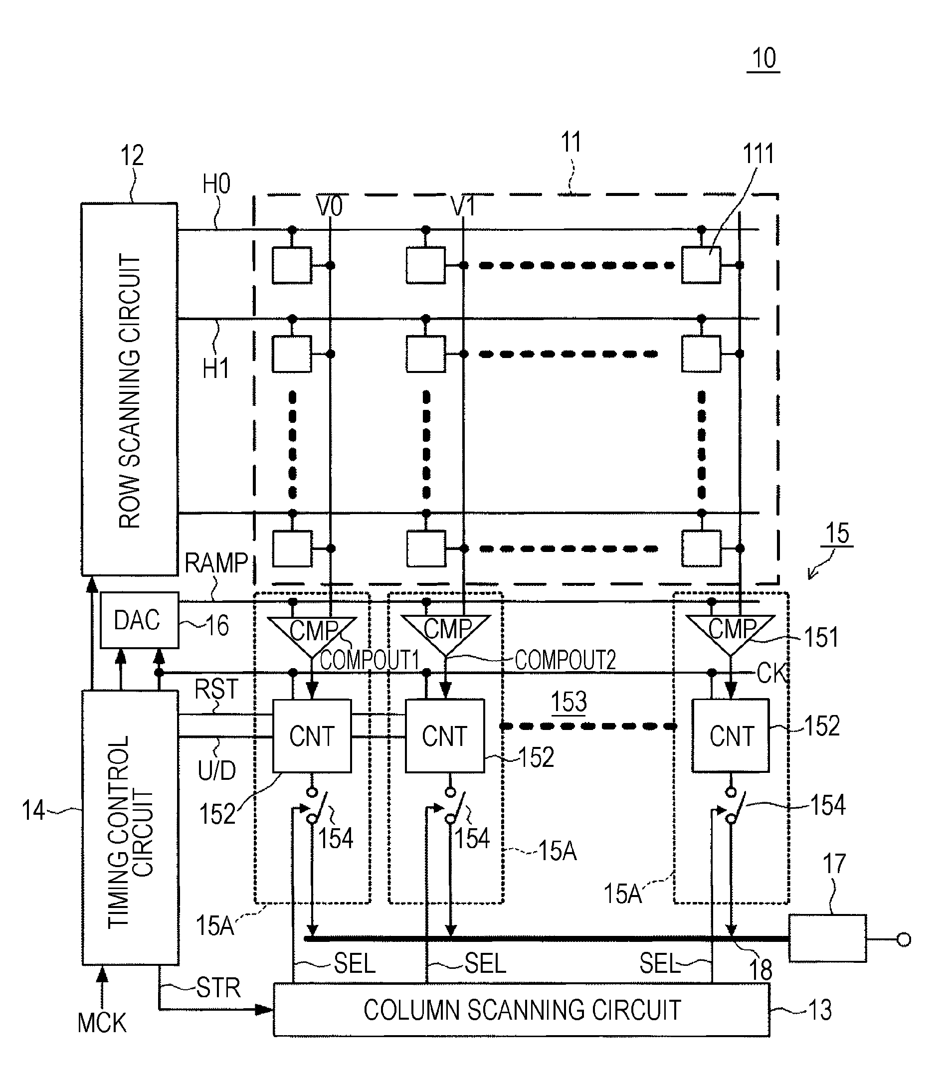
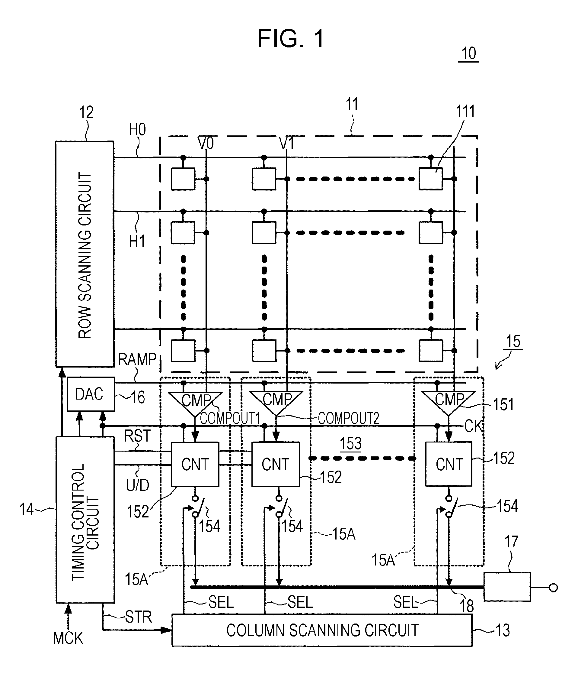
[0043]FIG. 1 is a block diagram showing an example of the configuration of a parallel column ADC-mounted solid-state image sensor (CMOS image sensor) including a data transfer circuit according to an embodiment of the present invention.

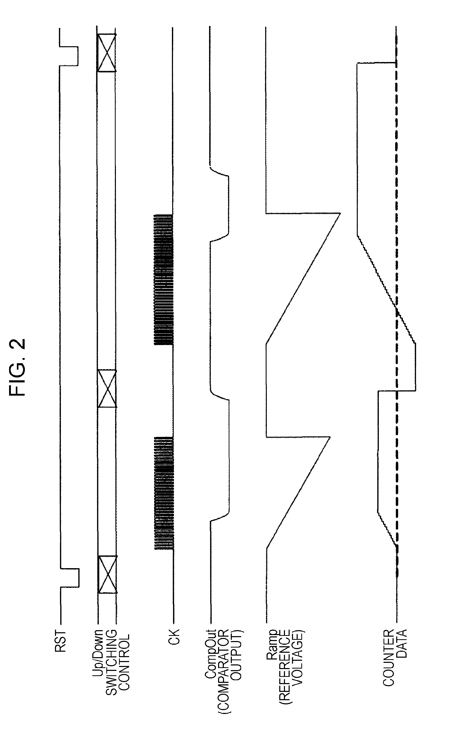
[0044]Furthermore, FIG. 2 shows operation waveforms of the solid-state image sensor of FIG. 1.

[0045]The solid-state image sensor 10 includes a pixel array unit 11 serving as an image-capturing unit, a row scanning circuit 12, a column scanning circuit 13, a timing control circuit 14, an ADC group 15, a digital-analog conversion circuit (hereinafter abbreviated as a “DAC (digital-analog converter)) 16 serving as a reference voltage generation circuit, and a data output circuit 17 having a sensing amplifier circuit (S / A), and the like.

[0046]The pixel array unit 11 is formed in such a manner that unit pixels 111 including a photodiode and an intra-pixel am...


PUM


Abstract

There are provided an A / D conversion circuit in which a counter is made to be capable of performing counting at both edges of a clock, up / down count values can be switched while the up / down count values are held, and the duty of the counting operation is difficult to be distorted even with the both-edge counting, a solid-state image sensor, and a camera system. An ADC 15A is configured as an integrating-type A / D conversion circuit using a comparator 151 and a counter 152. The counter 152 has a function of switching a count mode from an up count to a down count and from a down count to an up count while a value is held, a function of performing counting at both rising and falling edges of an input clock CK at a frequency two times as high as that of the input clock, and a function of latching the input clock CK in accordance with an output signal of the comparator 151 and setting non-inverted or inverted data of the latched data to be data of an LSB.

Description

TECHNICAL FIELD[0001]The present invention relates to an A / D conversion circuit that can be applied to parallel-column output-type CMOS image sensors or the like, a solid-state image sensor using the A / D conversion circuit, and a camera system.BACKGROUND ART[0002]In recent years, as solid-state image sensors taking the place of CCDs, CMOS image sensors have attracted attention.[0003]The reason for this is that various problems including the system becoming very complex because dedicated processes are necessary in the manufacture of CCD pixels, a plurality of power-supply voltages being necessary for the operations thereof, and furthermore, a plurality of peripheral ICs needing to be combined and operated, are overcome by using CMOS image sensors.[0004]For manufacturing CMOS image sensors, it is possible to use manufacturing processes that are the same as those used for typical CMOS-type integrated circuits, also driving using a single power source is possible, and furthermore, analo...

Claims


Application Information

Patent Timeline
Patent Type & Authority Patents(United States)
IPC IPC(8): H03M1/12H04N25/65H03M1/56H04N25/00
CPCH03K23/62H03M1/1023H03M1/1295H04N5/363H04N5/335H04N5/378H03M1/12H03M1/20H03M1/123H03M1/56H04N25/00H04N25/78H04N25/616H04N25/65H04N25/75
Inventor HISAMATSU, YASUAKI
Owner SONY CORP
Learn More