Liquid crystal lens structure and method of driving same
a liquid crystal lens and structure technology, applied in the direction of instruments, printers, cameras, etc., can solve the problems of difficult to easily reduce the manufacturing cost, the structure design and control precision of the zoom lens is difficult to achieve, and the electrode design is complicated. , the effect of high operating voltag
- Summary
- Abstract
- Description
- Claims
- Application Information
AI Technical Summary
Benefits of technology
Problems solved by technology
Method used
Image
Examples
first embodiment
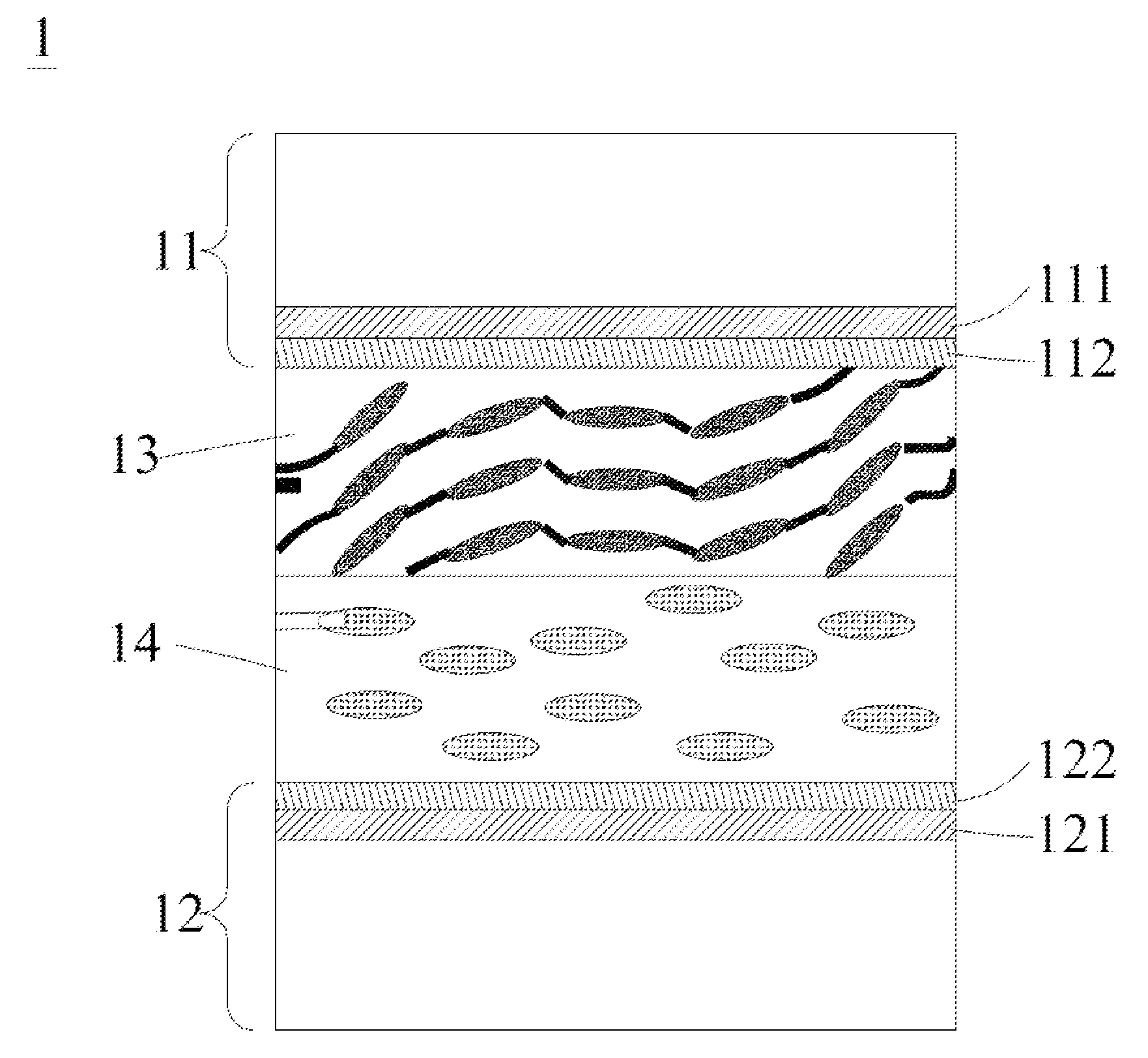
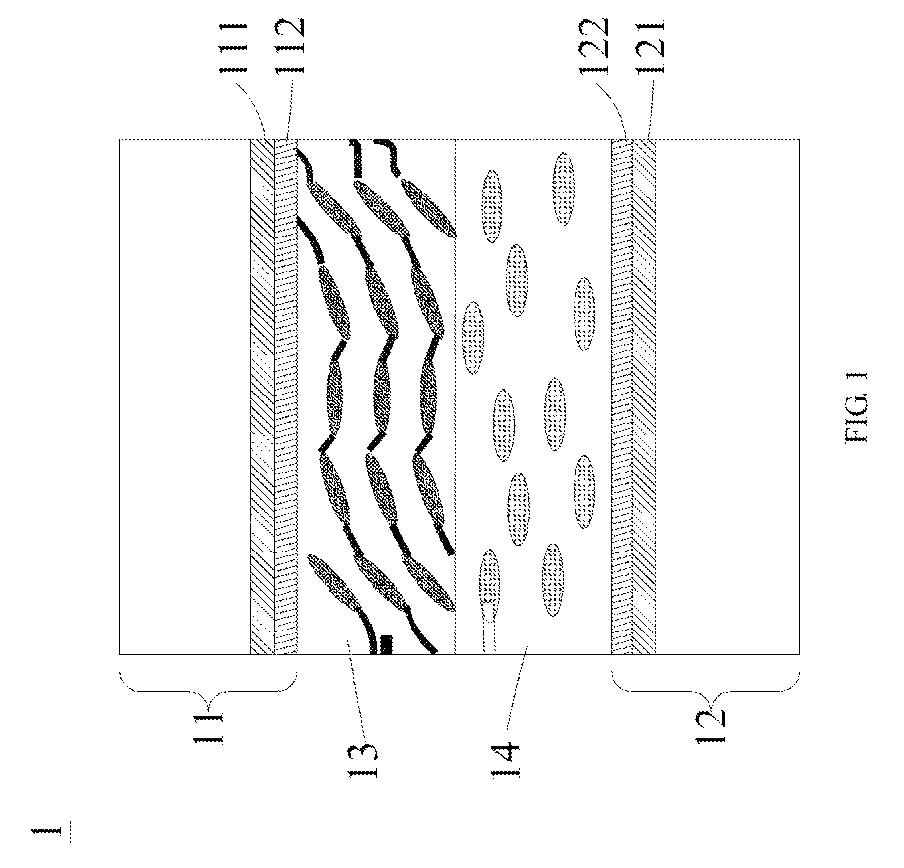
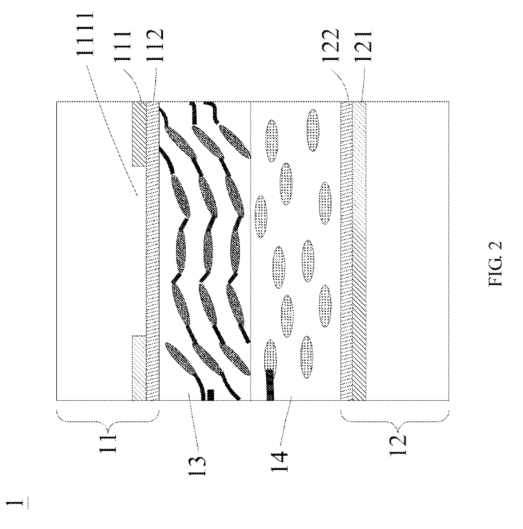
[0041]The present invention will now be described with some preferred embodiments thereof and with reference to the accompanying drawings. For the purpose of easy to understand, elements that are the same in the preferred embodiments are denoted by the same reference numerals. Please refer to FIG. 1 that is a conceptual view of a liquid crystal (LC) lens structure according to the present invention. As shown, the LC lens structure is generally denoted by reference numeral 1, and includes an upper substrate 11, a lower substrate 12, a liquid crystal and polymer composite film 13, and a liquid crystal (LC) layer 14.
[0042]The upper substrate 11 can have a first conductive layer 111 and a first alignment layer 112 provided thereon. The first conductive layer 111 is located at one side of the upper substrate 11, and the first alignment layer 112 is located at one side of the first conductive layer 111 opposite to the upper substrate 11. Similarly, the lower substrate 12 can have a second...
second embodiment
[0068]FIG. 9 is a graph showing the driving method according to the present invention.
[0069]First, an operating voltage of 35 Vrms is provided.
[0070]Then, the operating voltage is switched from 35 Vrms to 15 Vrms.
[0071]In the second embodiment of the driving method, the applied voltage is switched from a higher operating voltage to a lower operating voltage with a voltage fall time of 1 second.
third embodiment
[0072]Please refer to FIG. 10, which is a graph showing the driving method according to the present invention.
[0073]First, an operating voltage of 15 Vrms is provided.
[0074]Then, the operating voltage is switched from 15 Vrms to 55 Vrms.
[0075]Finally, the operating voltage is switched from 55 Vrms to 35 Vrms.
[0076]In the third embodiment of the driving method, a pulse of 55 Vrms with a pulse time of 298 ms is applied during the voltage rise time, in order to accelerate the reorientation of the liquid crystal molecules.
PUM
| Property | Measurement | Unit |
|---|---|---|
| diameter | aaaaa | aaaaa |
| dielectric constant | aaaaa | aaaaa |
| dielectric constant | aaaaa | aaaaa |
Abstract
Description
Claims
Application Information
 - R&D Engineer
- R&D Manager
- IP Professional
- Industry Leading Data Capabilities
- Powerful AI technology
- Patent DNA Extraction
Browse by: Latest US Patents, China's latest patents, Technical Efficacy Thesaurus, Application Domain, Technology Topic, Popular Technical Reports.
© 2024 PatSnap. All rights reserved.Legal|Privacy policy|Modern Slavery Act Transparency Statement|Sitemap|About US| Contact US: help@patsnap.com


