Micro device transfer head heater assembly and method of transferring a micro device

a technology of transfer head and heater, which is applied in the direction of layered products, lamination plant layout, chemical apparatus and processes, etc., can solve problems such as integration and packaging

Inactive Publication Date: 2013-01-08
APPLE INC
View PDF47 Cites 221 Cited by
  • Summary
  • Abstract
  • Description
  • Claims
  • Application Information

AI Technical Summary

Benefits of technology

[0008]A micro device transfer head and head array, and a method of transferring one or more micro devices to a receiving substrate are disclosed. For example, the receiving substrate may be, but is not limited to, a display substrate, a lighting substrate, a substrate with functional devices such as transistors or integrated circuits (ICs), or a substrate with metal redistribution lines.

Problems solved by technology

Integration and packaging issues are one of the main obstacles for the commercialization of micro devices such as radio frequency (RF) microelectromechanical systems (MEMS) microswitches, light-emitting diode (LED) display systems, and MEMS or quartz-based oscillators.

Method used


Image

  • Micro device transfer head heater assembly and method of transferring a micro device
  • Micro device transfer head heater assembly and method of transferring a micro device
  • Micro device transfer head heater assembly and method of transferring a micro device

Examples


Embodiment Construction

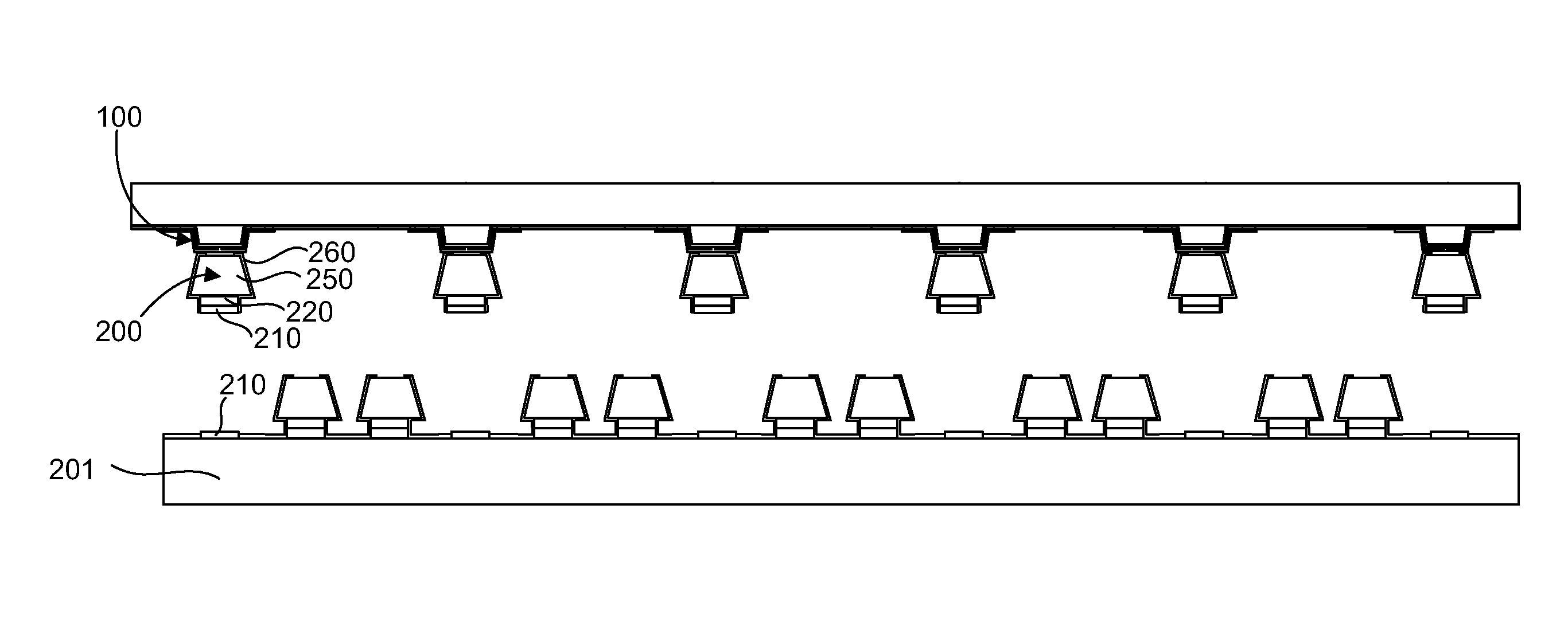
[0060]Embodiments of the present invention describe a micro device transfer head and head array, and method of transferring a micro device and an array of micro devices to a receiving substrate. For example, the receiving substrate may be, but is not limited to, a display substrate, a lighting substrate, a substrate with functional devices such as transistors or integrated circuits (ICs), or a substrate with metal redistribution lines. In some embodiments, the micro devices and array of micro devices described herein may be any of the micro LED device structures illustrated in FIGS. 19-21, and those described in related U.S. Provisional Application No. 61 / 561,706 and U.S. Provisional Application No. 61 / 594,919. While some embodiments of the present invention are described with specific regard to micro LEDs, it is to be appreciated that embodiments of the invention are not so limited and that certain embodiments may also be applicable to other micro devices such as diodes, transistor...


PUM

PropertyMeasurementUnit
temperatureaaaaaaaaaa

Abstract

A method of transferring a micro device and an array of micro devices are disclosed. A carrier substrate carrying a micro device connected to a bonding layer is heated to a temperature below a liquidus temperature of the bonding layer, and a transfer head is heated to a temperature above the liquidus temperature of the bonding layer. Upon contacting the micro device with the transfer head, the heat from the transfer head transfers into the bonding layer to at least partially melt the bonding layer. A voltage applied to the transfer head creates a grip force which picks up the micro device from the carrier substrate.

Description

RELATED APPLICATIONS[0001]This application claims the benefit of priority from U.S. Provisional Patent Application Ser. No. 61 / 561,706 filed on Nov. 18, 2011, U.S. Provisional Patent Application Ser. No. 61 / 594,919 filed on Feb. 3, 2012, U.S. Provisional Patent Application Ser. No. 61 / 597,109 filed on Feb. 9, 2012 and U.S. Provisional Patent Application Ser. No. 61 / 597,658 filed on Feb. 10, 2012, the full disclosures of which are incorporated herein by reference.BACKGROUND[0002]1. Field[0003]The present invention relates to micro devices. More particularly embodiments of the present invention relate to a method of transferring one or more micro devices to a receiving substrate with a micro device transfer head.[0004]2. Background Information[0005]Integration and packaging issues are one of the main obstacles for the commercialization of micro devices such as radio frequency (RF) microelectromechanical systems (MEMS) microswitches, light-emitting diode (LED) display systems, and MEMS...

Claims


Application Information

Patent Timeline
Patent Type & Authority Patents(United States)
IPC IPC(8): B29C65/02B29C65/48B32B37/04B32B39/00B32B43/00
CPCH01L21/67B32B38/18H01L24/83H01L24/97Y10T156/1707H01L2924/14H01L2224/83005H01L2224/97H01L21/67144Y10T156/1744Y10T156/1749Y10T156/1153Y10T156/17Y10T156/1776H01L2924/12041H01L2924/1461Y10T156/1705Y10T156/1911H01L2224/83H01L2924/00H01L24/75H01L2924/10253H01L2924/10329H01L2924/1421H01L2924/1431H01L2924/1434H01L2224/75725H01L2924/12042H01L24/95H01L2224/7598H01L2221/68368H01L2224/95001H01L21/67712H01L21/67733H01L25/0753H01L29/167H01L33/62H01L2933/0066H01L2224/75252
Inventor BIBL, ANDREASHIGGINSON, JOHN A.LAW, HUNG-FAI STEPHENHU, HSIN-HUA
Owner APPLE INC
Why Eureka
Try Eureka