Supercharge Your Innovation With Domain-Expert AI Agents!

High voltage device with reduced leakage

a high-voltage device and leakage technology, applied in the field of semiconductor devices, can solve the problems of high leakage problems, increase the complexity of processing and manufacturing ics, and the incorporation of high-voltage devices

Active Publication Date: 2013-01-08
TAIWAN SEMICON MFG CO LTD
View PDF3 Cites 24 Cited by
  • Summary
  • Abstract
  • Description
  • Claims
  • Application Information

AI Technical Summary

Benefits of technology

The solution effectively reduces off-state current (leakage) and enhances time-dependent dielectric breakdown reliability, improving DC performance and hot carrier injection lifetime, while being compatible with logic device fabrication processes, thus maintaining low costs for System on Chip (SoC) technology.

Problems solved by technology

However, these advances have increased the complexity of processing and manufacturing ICs and, for these advances to be realized, similar developments in IC processing and manufacturing are needed.
As semiconductor circuits composed of devices such as metal-oxide-semiconductor field effect transistors (MOSFETs) are adapted for high voltage applications, problems arise with respect to incorporating a high voltage device with a low voltage device (e.g., a logic device) for a system on chip (SoC) technology.
For example, as the scaling down of logic device continues with advanced technologies (e.g., 45 nm and below), the process flow may be accompanied with high implantation concentration to prevent punch-through between source and drain or to reduce resistance of source and drain, and thus may cause high leakage problems and the degradation of device reliability.

Method used


Image

  • High voltage device with reduced leakage
  • High voltage device with reduced leakage
  • High voltage device with reduced leakage

Examples


Embodiment Construction

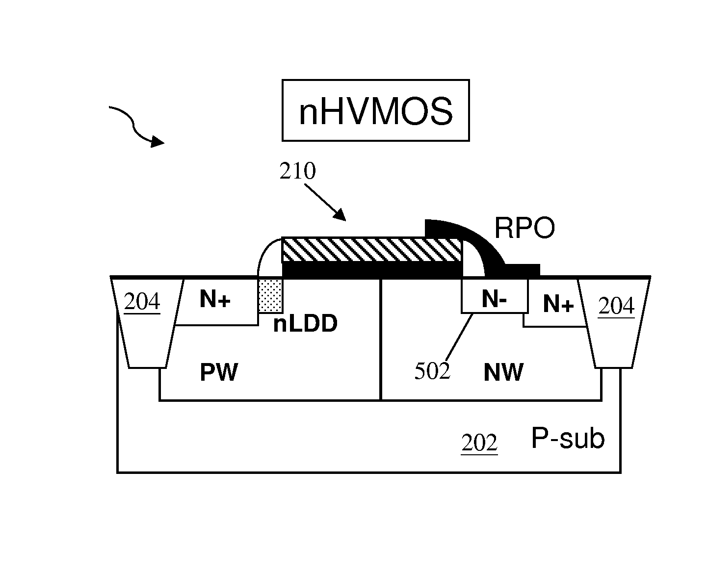
[0015]The present disclosure relates generally to the field of semiconductor integrated circuits. It is understood that the following disclosure provides many different embodiments, or examples, for implementing different features of the invention. Specific examples of components and arrangements are described below to simplify the present disclosure. These are, of course, merely examples and are not intended to be limiting. In addition, the present disclosure may repeat reference numerals and / or letters in the various examples. This repetition is for the purpose of simplicity and clarity and does not in itself dictate a relationship between the various embodiments and / or configurations discussed. Moreover, the formation of a first feature over or on a second feature in the description that follows may include embodiments in which the first and second features are formed in direct contact, and may also include embodiments in which additional features may be formed interposing the fi...


PUM


Abstract

A semiconductor device is provided which includes a semiconductor substrate, a gate structure formed on the substrate, sidewall spacers formed on each side of the gate structure, a source and a drain formed in the substrate on either side of the gate structure, the source and drain having a first type of conductivity, a lightly doped region formed in the substrate and aligned with a side of the gate structure, the lightly doped region having the first type of conductivity, and a barrier region formed in the substrate and adjacent the drain. The barrier region is formed by doping a dopant of a second type of conductivity different from the first type of conductivity.

Description

PRIORITY DATA[0001]This application claims priority to Provisional Application Ser. No. 61 / 092,993 filed on Aug. 29, 2008, entitled “High Voltage Device With Reduced Leakage,” the entire disclosure of which is incorporated herein by reference.BACKGROUND[0002]The present disclosure relates generally to semiconductor technology, and more particularly, to a high voltage device with reduced leakage and method of making the same.[0003]The semiconductor integrated circuit (IC) industry has experienced rapid growth. Technological advances in IC materials and design have produced generations of ICs where each generation has smaller and more complex circuits than the previous generation. However, these advances have increased the complexity of processing and manufacturing ICs and, for these advances to be realized, similar developments in IC processing and manufacturing are needed.[0004]As semiconductor circuits composed of devices such as metal-oxide-semiconductor field effect transistors (...

Claims


Application Information

Patent Timeline
Patent Type & Authority Patents(United States)
IPC IPC(8): H01L29/78
CPCH01L29/0634H01L29/0646H01L29/0847H01L29/7802H01L29/66659H01L29/7835H01L29/665H01L29/1045
Inventor CHUNG, SHU-WEI VANESSAYU, KUO-FENG
Owner TAIWAN SEMICON MFG CO LTD
Features
  • R&D
  • Intellectual Property
  • Life Sciences
  • Materials
  • Tech Scout
  • Unparalleled Data Quality
  • Higher Quality Content
  • 60% Fewer Hallucinations
Learn More