Method of transferring device

a technology of transferring device and surface, which is applied in the direction of layered products, chemistry apparatus and processes, manufacturing tools, etc., can solve the problems of difficult control of device scattering direction and a lot of trouble in processing the surface of the device, and achieve the effect of accurately transferring the device onto the second substra

Active Publication Date: 2013-01-29
SONY CORP
View PDF3 Cites 38 Cited by
  • Summary
  • Abstract
  • Description
  • Claims
  • Application Information

AI Technical Summary

Benefits of technology

[0007]Thus, it is desirable to provide a method of transferring a device capable of accurately transferring a device onto a second substrate arranged apart without processing the surface of the device.
[0010]As a result, according to the embodiment of the invention, it is possible to accurately transfer a device onto the second substrate without processing the surface of the device.

Problems solved by technology

With the above-described method, however, it takes a lot of trouble to process the surface of the device onto which the laser beam is irradiated in advance so as to accurately transfer a device onto the second substrate arranged apart.
In addition, when the surface of the device should be maintained flat, it is difficult to control the device scattering direction.

Method used


Image

  • Method of transferring device
  • Method of transferring device
  • Method of transferring device

Examples


first embodiment

1. First Embodiment

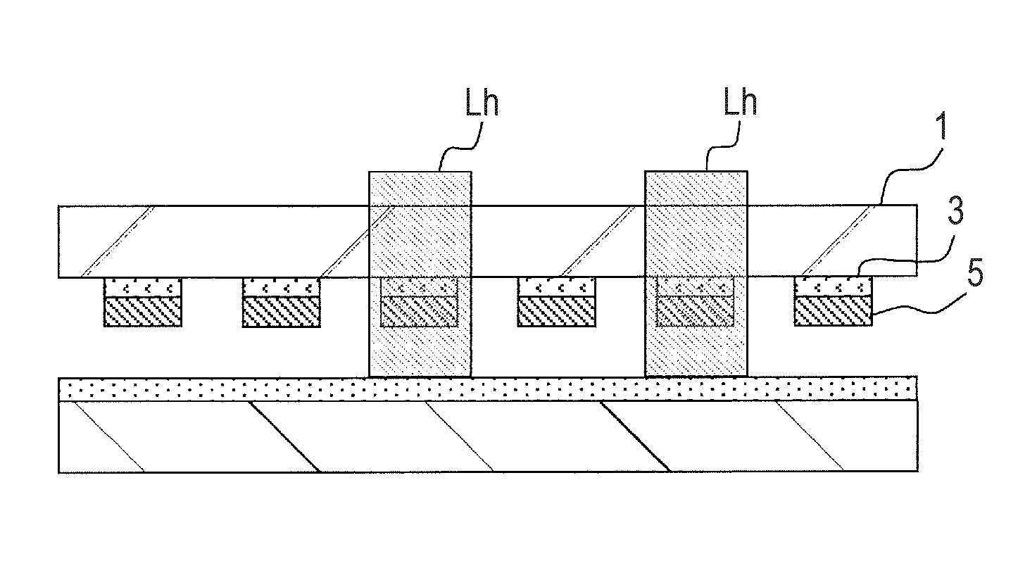
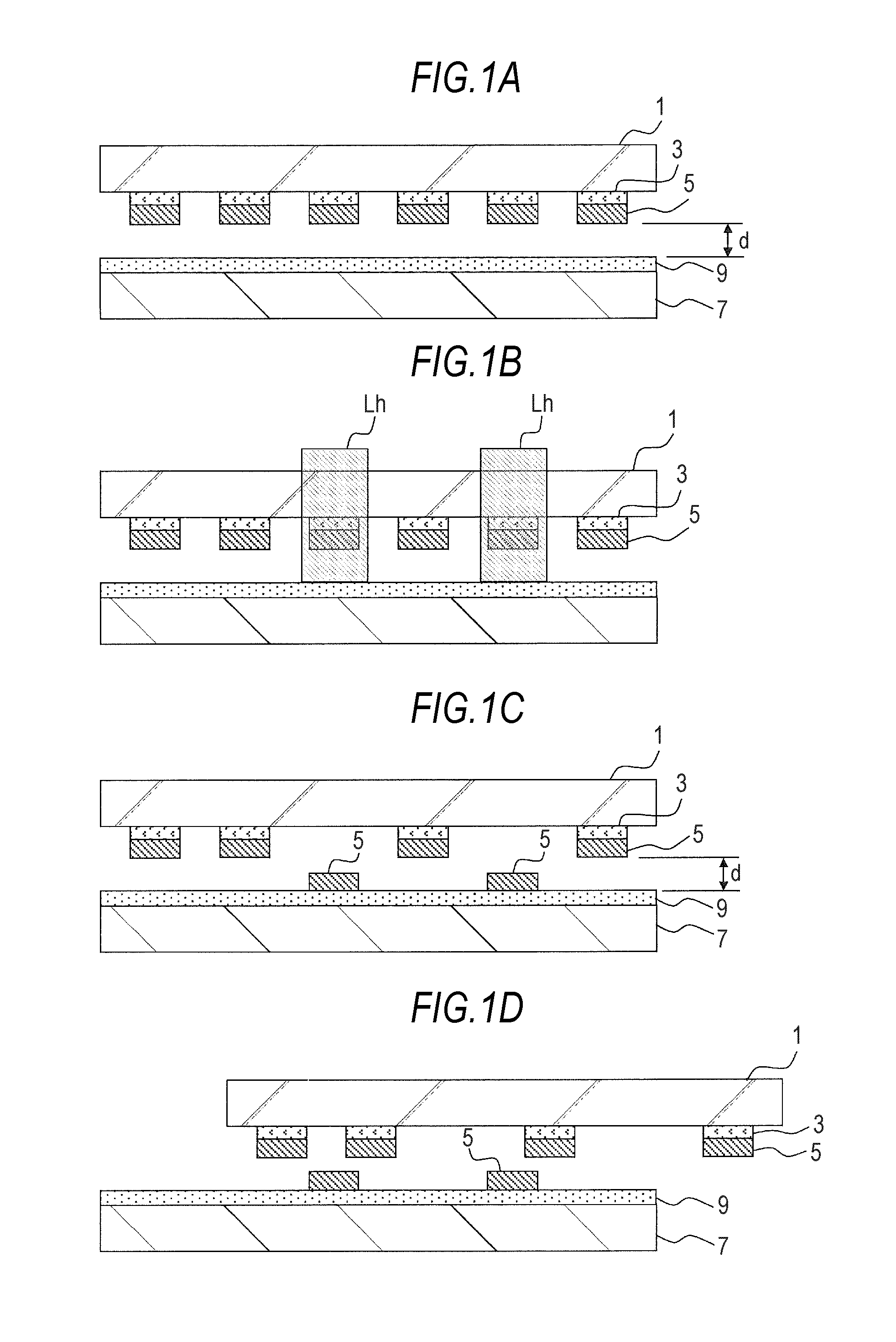
[0028]FIGS. 1A to 1D are sectional process views illustrating a method of transferring a device to which the invention is applied. A method of transferring a device described herein is, for example, a method of transferring an LED device from a first substrate onto a second substrate in a manufacturing process or the like of a display device in which light-emitting diodes (LEDs) are arranged in a matrix. This method is carried out as follows.

[0029]First, as shown in FIG. 1A, a plurality of devices 5 are placed on a first substrate 1 with a release layer 3 interposed therebetween. An adhesive layer 9 is provided on a second substrate 7.

[0030]The first substrate 1 is, for example, a substrate for holding devices constituting a display device. The first substrate 1 is made of a material which is nonabsorbent to a laser beam used in the transfer method as well as such a material that the devices 5 on the first substrate 1 can be observed through the first substrate 1 ...

second embodiment

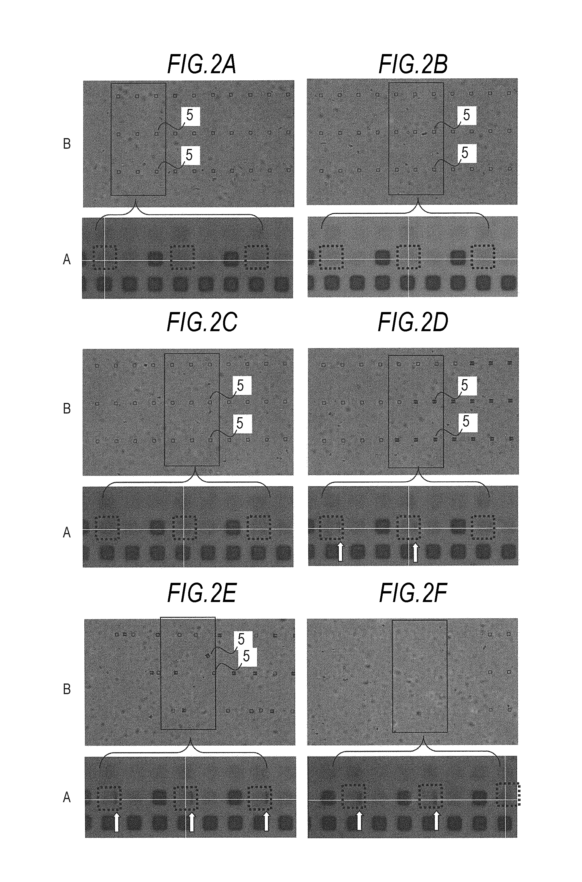
[0062]A repair method of transferring a device with respect to a device absent part of a second substrate from a first substrate will be described as a second embodiment with reference to FIGS. 3A to 4D.

[0063]As shown in a plan view of FIG. 3A and a sectional view of FIG. 3B [corresponding to a section taken along the line A-A′ of FIG. 3A], devices 5 are transferred onto a second substrate 7 in a predetermined arrangement by the procedure of the first embodiment or other procedures. In this state, a device absent part B where a device 5 has failed to be transferred exists on the second substrate 7, and the device 5 is transferred with respect to a device absent part B such that a repair is carried out.

[0064]In this case, first, as shown in FIG. 4A, a new first substrate 1 on which devices 5 for a repair are mounted is arranged to be opposite a second substrate 7 on which a plurality of devices 5 are already transferred. In this case, similarly to the first embodiment, the first subs...

third embodiment

[0073]A first example where arrangement on a first substrate is changed and devices are rearranged on a second substrate will be described as a third embodiment with reference to FIGS. 5 and 6. In this case, description will be provided for the transfer when the characteristics of device columns are averaged.

[0074]FIG. 5 shows a state where a plurality of light-emitting devices 5 are mounted on the first substrate 1 with a light-emission intensity distribution. Such a light-emission intensity distribution results from a distribution on a wafer on which light-emitting devices 5 are formed.

[0075]In this case, first, as shown in FIG. 6A(1), the devices 5 which are alternately arranged are transferred from the first substrate 1 to a first transfer range A on the second substrate. Next, as shown in FIG. 6A(2), second transfer is carried out in a nested shape from the first substrate to the second substrate at a position where the transfer range is moved in the horizontal direction so as ...


PUM

PropertyMeasurementUnit
areaaaaaaaaaaa
shapeaaaaaaaaaa
thicknessaaaaaaaaaa

Abstract

A method of transferring a device includes the steps of: arranging a first substrate, on which a device is provided with a release layer having a planar shape equal to or smaller than the device interposed therebetween, and a second substrate, on which an adhesive layer is provided, so as to be spaced from and opposite each other in a state where the device and the adhesive layer face each other; and irradiating a laser beam having an irradiation area larger than the base area of the release layer onto the entire surface of the release layer from the first substrate side so as to ablate the release layer, to separate the device from the first substrate, and to transfer the device on the second substrate.

Description

BACKGROUND OF THE INVENTION[0001]1. Field of the Invention[0002]The present invention relates to a method of transferring a device, and in particular, to a method of transferring a device from a first substrate onto a second substrate by a laser ablation technique.[0003]2. Description of the Related Art[0004]As a method of selectively and accurately transferring part of a group of devices arranged on a first substrate onto a second substrate, there is an attempt for application of a laser ablation technique. Device transfer using a laser ablation technique is carried out as follows. First, the first substrate and the second substrate are arranged such that the device arrangement surface of the first substrate and the adhesive layer forming surface of the second substrate face each other. In this state, a laser beam is irradiated only onto a position corresponding to a device to be transferred from the first substrate side. Thus, a release layer provided between the first substrate a...

Claims


Application Information

Patent Timeline
Patent Type & Authority Patents(United States)
IPC IPC(8): H01L21/82H01L21/02H01L27/12H01L33/48
CPCH01L21/268H01L21/6835H01L24/83H01L24/95H01L33/0079H01L2924/12041H01L2221/68322H01L2221/68359H01L2224/83192H01L2224/838H01L2924/01033H01L2924/01057H01L2924/19043H01L2924/3025H01L2924/01005H01L2924/01006H01L2924/00H01L2224/83005H01L33/0093
Inventor MIZUNO, TAKESHITOMODA, KATSUHIROOOHATA, TOYOHARU
Owner SONY CORP
Why Eureka
Try Eureka