Semiconductor device and method of manufacturing the same
a technology of semiconductor devices and semiconductors, applied in the direction of semiconductor devices, basic electric elements, electrical equipment, etc., can solve the problems of difficulty in electrodes have arisen, and the difficulty of avoiding the increase of schottky barrier between a p-type region and an n-type region, so as to reduce the number of steps in the manufacturing process, the effect of sufficiently suppressing the increase in contact resistan
- Summary
- Abstract
- Description
- Claims
- Application Information
AI Technical Summary
Benefits of technology
Problems solved by technology
Method used
Image

Examples
first embodiment
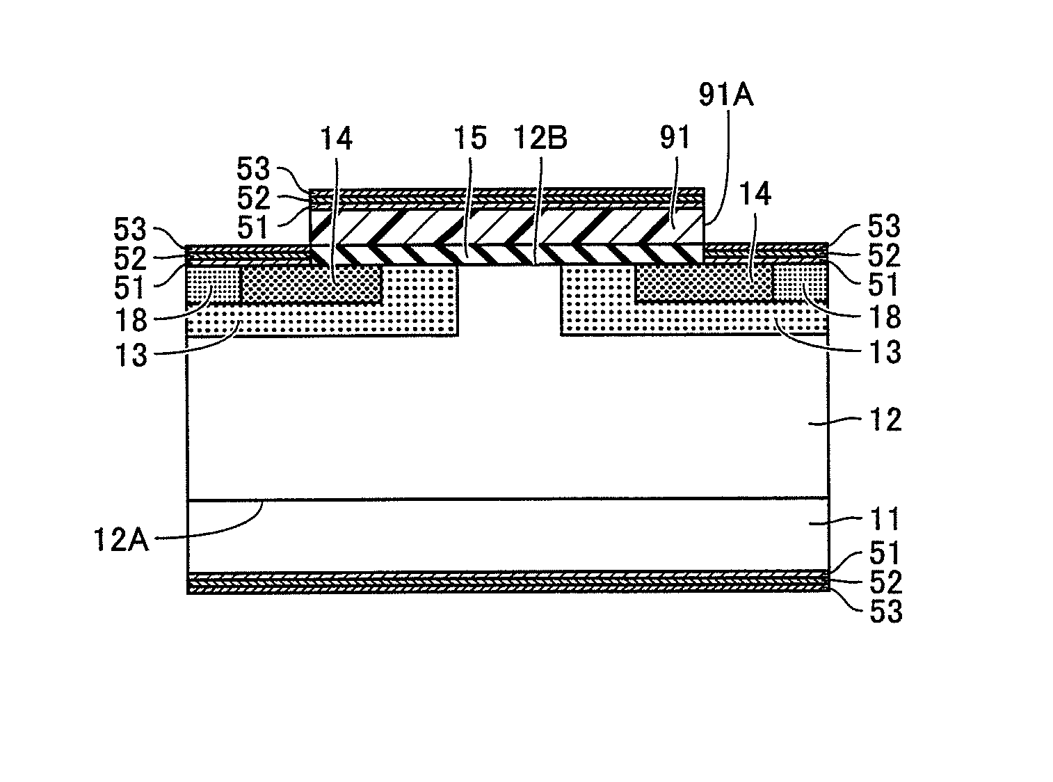
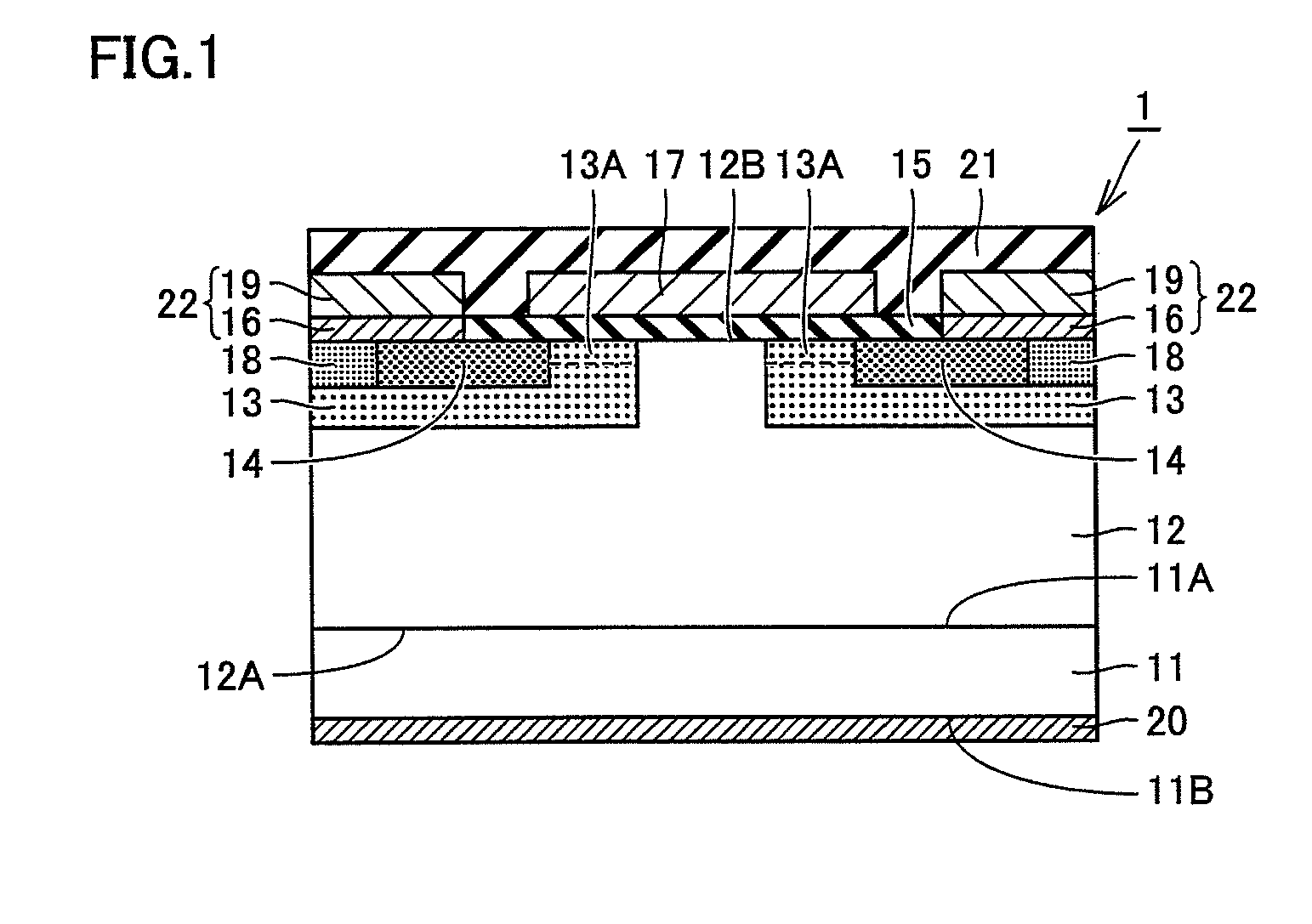
[0078]Initially, a MOSFET in the first embodiment will be described. Referring to FIG. 1, a MOSFET 1 in the first embodiment includes an n+ SiC substrate 11 being a substrate composed of silicon carbide (SiC) and having an n conductivity type (a first conductivity type), an n− SiC layer 12 serving as a semiconductor layer composed of SiC and having the n conductivity type (the first conductivity type), a pair of p bodies 13 serving as second-conductivity-type regions having a p conductivity type (a second conductivity type), an n+ source region 14 serving as a high-concentration first-conductivity-type region having the n conductivity type (the first conductivity type), and a p+ region 18 serving as a high-concentration second-conductivity-type region having the p conductivity type (the second conductivity type). N+ SiC substrate 11 contains an n-type impurity (an impurity having the n conductivity type) such as N (nitrogen) at high concentration.
[0079]N− SiC layer 12 is formed on o...
second embodiment
[0110]A second embodiment representing another embodiment of the present invention will now be described. Referring to FIG. 10, a JFET 3 which is a junction field effect transistor representing a semiconductor device in the second embodiment is the same as MOSFET 1 in the first embodiment in a structure of an ohmic contact electrode and achieves similar effects. Specifically, JFET 3 includes an n-type substrate 31 composed of SiC and having the n conductivity type, a first p-type layer 32 formed on n-type substrate 31, an n-type layer 33 formed on first p-type layer 32, and a second p-type layer 34 formed on n-type layer 33. Here, the p-type layer and the n-type layer are layers composed of SiC and having the p and n conductivity types, respectively. In addition, for example, first p-type layer 32 can have a thickness of approximately 10 μm and concentration of a p-type impurity of approximately 7.5×1015 cm−3. For example, n-type layer 33 can have a thickness of approximately 0.45 μ...
third embodiment
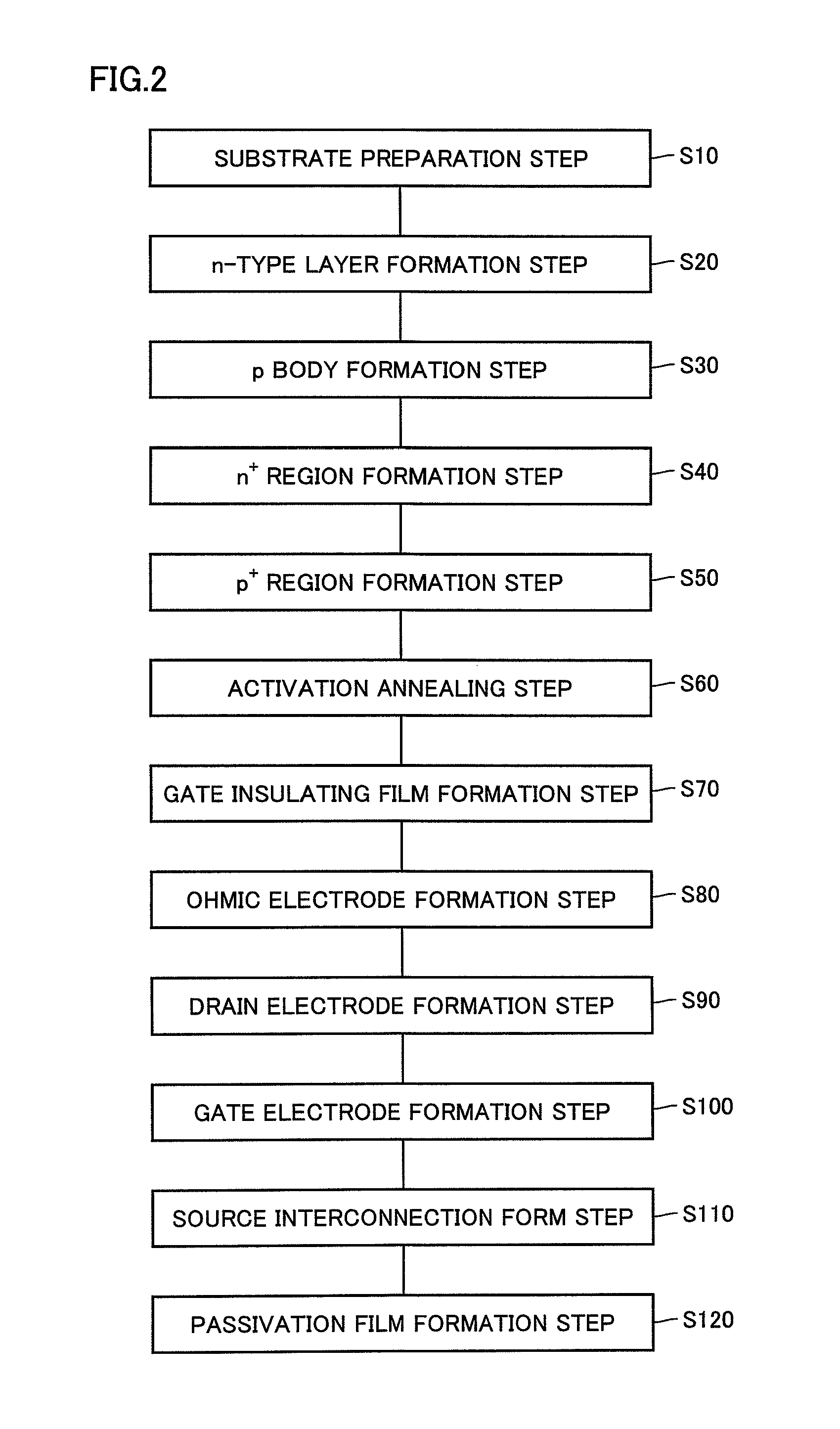
[0135]A third embodiment representing yet another embodiment of the present invention will now be described. A semiconductor device in the third embodiment is basically structured similarly to MOSFET 1 representing the semiconductor device in the first embodiment, achieves similar effects, and can be manufactured similarly. A method of manufacturing MOSFET 1 in the third embodiment is different from that in the first embodiment in an ohmic electrode formation step and a drain electrode formation step (see FIG. 2).
[0136]Namely, referring to FIGS. 19, 2 and 3, an ohmic contact electrode formation step (S80) in the third embodiment is different from that in the first embodiment in that a Pt film formation step is performed as a step (S85) after the Si film formation step (S83) and before the alloying step (S84). Specifically, in the ohmic electrode formation step (S80) and the drain electrode formation step (S90) in the third embodiment, initially, the steps (S81) to (S83) are performe...
PUM
 Abstract
Description
Claims
Application Information
 - R&D
- Intellectual Property
- Life Sciences
- Materials
- Tech Scout
- Unparalleled Data Quality
- Higher Quality Content
- 60% Fewer Hallucinations
Browse by: Latest US Patents, China's latest patents, Technical Efficacy Thesaurus, Application Domain, Technology Topic, Popular Technical Reports.
© 2025 PatSnap. All rights reserved.Legal|Privacy policy|Modern Slavery Act Transparency Statement|Sitemap|About US| Contact US: help@patsnap.com