Photoelectric converting film stack type solid-state image pickup device, and method of producing the same

Active Publication Date: 2005-12-01
FUJIFILM CORP
View PDF2 Cites 57 Cited by
  • Summary
  • Abstract
  • Description
  • Claims
  • Application Information

AI Technical Summary

Benefits of technology

[0034] According to the configuration, the production cost of the whole photoele

Problems solved by technology

In the related-art solid-state image pickup device, therefore, many light receiving portions and signal read circuits must be formed on the same surface of a semiconductor substrate, thereby producing a problem in that the area for the light receiving portions cannot be increased.
This causes a false color, and reduces the resolution.
Furthermore, blue light and green light incident on a light receiving portion where a red color filter is formed do not contribute to photoelectric conversion, but are absorbed as heat into the color filter, thereby producing another problem in that the light use efficiency is poor and the sensitivity is low.
As described above, the related-art solid-state image pickup device has various problems.
Consequently, a CCD device and a CMOS device are hardly expected to configure an image sensor which can solve the above-discussed problems, and which is superior in image quality and sensitivity than the related-ar

Method used


Image

  • Photoelectric converting film stack type solid-state image pickup device, and method of producing the same
  • Photoelectric converting film stack type solid-state image pickup device, and method of producing the same
  • Photoelectric converting film stack type solid-state image pickup device, and method of producing the same

Examples


first embodiment

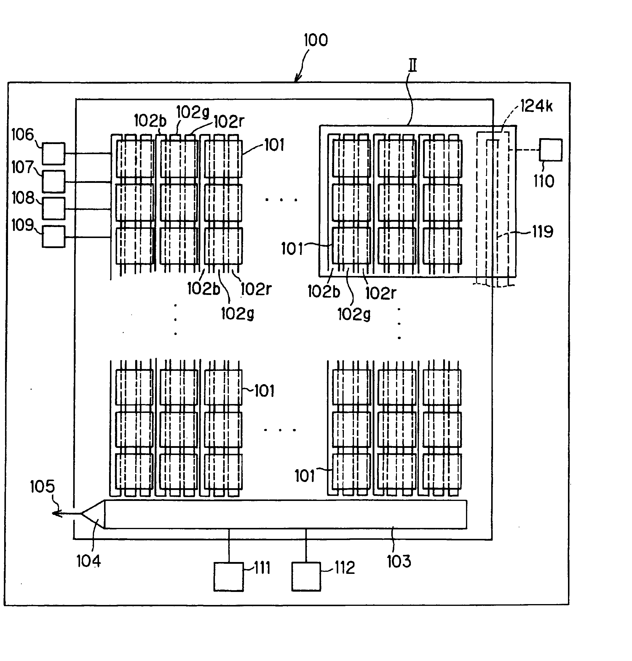
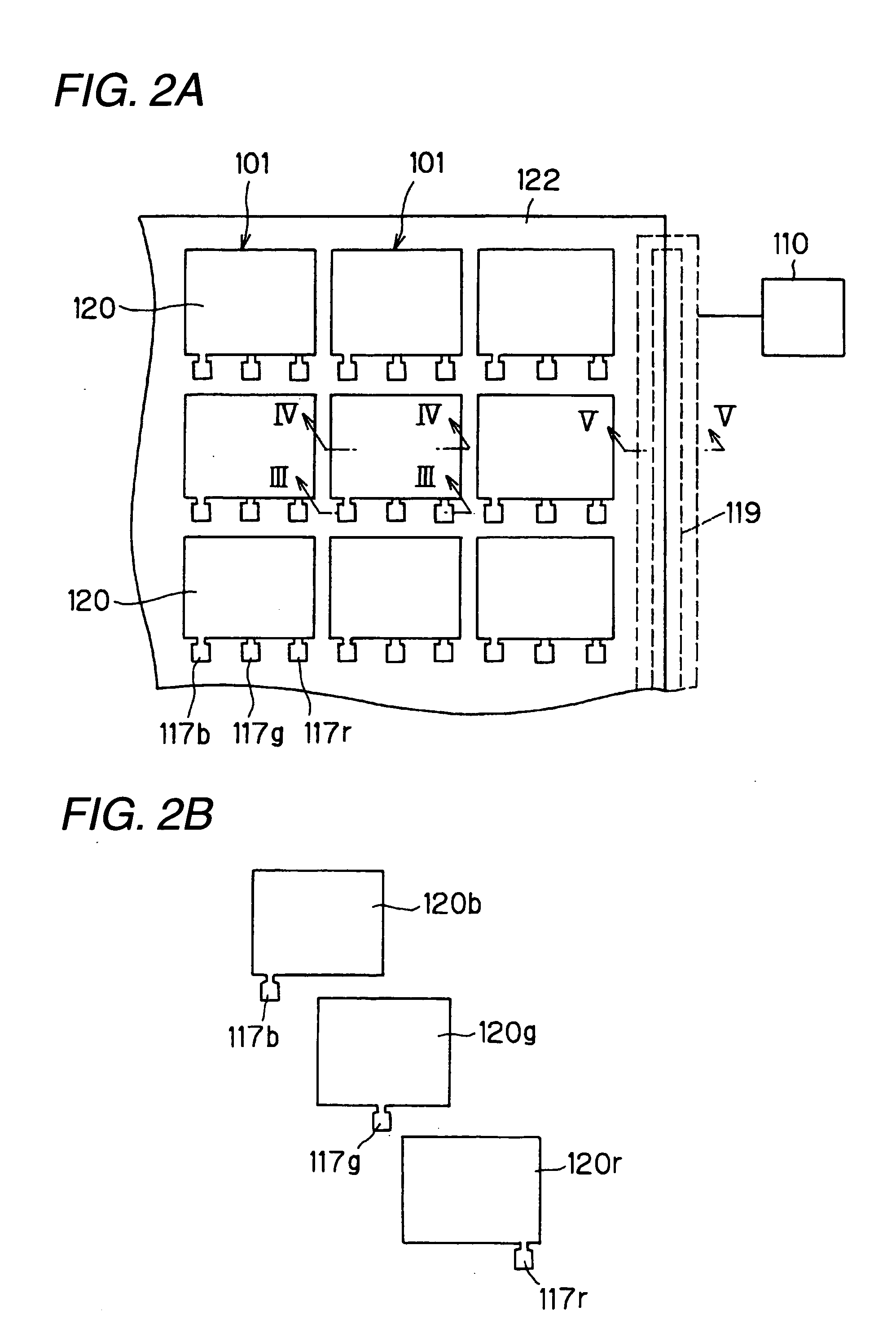
[0063]FIG. 1 is a surface diagram of a photoelectric converting film stack type solid-state image pickup device of a first embodiment of the invention. In the photoelectric converting film stack type solid-state image pickup device 100, many light receiving portions (pixels) 101 are arranged, in this example, vertically and horizontally or in a lattice manner.

[0064] On the surface of a semiconductor substrate which is disposed below the light receiving portions 101 of the photoelectric converting film stack type solid-state image pickup device 100, three vertical transfer paths (column CCD registers) 102b, 102g, 102r (the suffixes b, g, r correspond to blue (B), green (G), and red (R), respectively, and the same shall apply hereinafter) are formed in correspondence with the light receiving portions 101 which are arranged in the column direction, respectively. A horizontal transfer path (row CCD register) 103 is formed in a lower side edge of the semiconductor substrate.

[0065] An a...

second embodiment

[0103]FIGS. 21A and 21B are cross-sectional diagrams of a photoelectric converting film stack type solid-state image pickup device of a second embodiment of the invention, and FIGS. 22A and 22B are cross-sectional diagrams showing the middle of the production of the device. In the figures, “A” is a cross-sectional diagram taken at the same position as FIG. 3, and “B” is a cross-sectional diagram taken at the same position as FIG. 5 in the same manner as FIGS. 6A and 6B to 20A and 20B.

[0104]FIGS. 22A and 22B are diagrams showing a production procedure after the production step of FIGS. 11A and 11B in the first embodiment. In the first embodiment, after the step of FIGS. 11A and 11B in which the conductive film 151 is patterned, the photoelectric converting film 121r is stacked as shown in FIGS. 12A and 12B. When the conductive film 151 is patterned to form the conductive films 116g, 116b, the pad 117b and the pixel electrode film 120b, a step difference is formed in an end of each f...

third embodiment

[0107]FIGS. 23A and 23B are cross-sectional diagrams of a photoelectric converting film stack type solid-state image pickup device of a third embodiment of the invention, and FIGS. 24A and 24B to 26A and 26B are diagrams showing the middle of the production of the device. In the figures, “A” is a cross-sectional diagram taken at the same position as FIG. 3, and “B” is a cross-sectional diagram taken at the same position as FIG. 5 in the same manner as FIGS. 6A and 6B to 20A and 20B.

[0108] In the first and second embodiments, as shown in, for example, FIG. 5, the longitudinal line 143-2 is connected to the longitudinal line 143-3 through the conductive film 120k-2. The conductive film 120k-2 is formed by patterning the conductive film for forming the pixel electrode film 120g. As described in the second embodiment, preferably, the pixel electrode film is thin because asperities of the photoelectric converting film are suppressed. When the pixel electrode film is thin, however, also ...


PUM


Abstract

A solid-state image pickup device comprises: a plurality of photoelectric converting films stacked via an insulating layer, the photoelectric converting films being above a semiconductor substrate in which a signal read circuit is formed, in which each of the photoelectric converting films is sandwiched between a pixel electrode film and an opposing electrode film, wherein the pixel electrode film of an upper one of the photoelectric converting films is connected to the signal read circuit by a longitudinal line passing through a lower one of the photoelectric converting films, and, in the longitudinal line, a passing portion which passes through the lower photoelectric converting film is formed by filling an opening with a conductive material, the opening being formed from a same plane of the pixel electrode film stacked on the lower photoelectric converting film to an upper end face of the insulating layer stacked above the photoelectric converting film.

Description

BACKGROUND OF THE INVENTION [0001] 1. Field of the Invention [0002] The present invention relates to a photoelectric converting film stack type solid-state image pickup device in which a plurality of photoelectric converting films that generate charges corresponding to the amount of received light are stacked on a semiconductor substrate, and more particularly to a photoelectric converting film stack type solid-state image pickup device in which the number of production steps is decreased, the performance is improved, and the production cost is reduced, and a method of producing such a device. [0003] 2. Description of the Related Art [0004] In a CCD solid-state image pickup device or a CMOS solid-state image pickup device which is mounted on a digital camera, a large number of photoelectric converting elements (photodiodes) serving as light receiving portions, and signal read circuits which read out photoelectric conversion signals obtained in the photoelectric converting elements a...

Claims


Application Information

Patent Timeline
IPC IPC(8): H01L27/146H01L29/04H01L31/10
CPCH01L27/14609H01L27/14687H01L27/14647H01L27/14636
Inventor SUZUKI, NOBUO
Owner FUJIFILM CORP
Why Eureka
Try Eureka