Solid-state imaging device and method for making the same, and imaging apparatus

a solid-state imaging and imaging device technology, applied in the direction of solid-state devices, color television, television systems, etc., can solve the problems of difficult filling, difficult to form the surface by etching, and the difficulty of controlling the radius of curvature of the lens by both methods, so as to facilitate the control of the inner lens' lens shape, improve the degree of focusing incident light, and improve the effect of sensitivity

Active Publication Date: 2013-02-26
SONY SEMICON SOLUTIONS CORP
View PDF19 Cites 3 Cited by
  • Summary
  • Abstract
  • Description
  • Claims
  • Application Information

AI Technical Summary

Benefits of technology

[0012]It is desirable to facilitate control of the lens shape and provide a solid-state imaging device that can be manufactured easily and exhibits good characteristics, such as high sensitivity, and a method for making such a solid-state imaging device. It is also desirable to provide an imaging apparatus including the solid-state imaging device.
[0017]Since the film formed in the outer part of the interior of the hole in the insulating layer is formed by a coating technique, a curved surface, which forms a lens surface, can be easily formed at the bottom of the hole by the surface tension that occurs due to coating.
[0018]Since a lens surface is formed by the interface between the core and the film formed by the coating technique at the bottom of the hole and the inner lens is integrated with the waveguide, the incident light can be focused by the lens surface and guided into the light receiving unit. As a result, the degree at which the light is focused on the light receiving unit can be increased and more incident light can be introduced into the light receiving unit.
[0022]According to embodiments of the present invention, the degree of focusing incident light can be increased by the functions of the waveguide and the inner lens and more incident light can be guided into the light receiving unit. Thus, the sensitivity can be improved.
[0023]Moreover, since the film that constitutes the cladding of the waveguide together with the insulating layer is formed by coating, a lens shape for the inner lens can be easily formed at the bottom of the waveguide. Accordingly, the control of the lens shape of the inner lens can be facilitated and the solid-state imaging device can be easily made. Moreover, the waveguide and the inner lens can be simultaneously formed to be integrated with each other and the number of process steps can be decreased compare to when the waveguide and the inner lens are formed separately.
[0024]According to the imaging apparatus of the embodiment, since the sensitivity of the solid-state imaging device is improved, signals can be sufficiently obtained by photoelectric conversion in the solid-state imaging device. Thus, images can be captured in a relatively dark location. Therefore, an imaging apparatus that has high sensitivity and can capture images in a relatively dark location can be realized.

Problems solved by technology

However, both methods have a difficulty of controlling the radius of curvature of the lens.
However, according to this method, it is difficult to fill the shape as the pattern becomes finer and the nitride film formed in other regions has to be removed.
Moreover, Although one surface of the inner lens remote from the light receiving unit is desirably flat or convex in shape, such a surface is difficult to form by etching.
A chemical mechanical polishing (CMP) technique may be used but has a difficulty of controlling the polishing rate.
Thus, it has been difficult to obtain a desired lens shape.
Thus, the number of steps of device production tends to increase and the cost also tends to rise.

Method used


Image

  • Solid-state imaging device and method for making the same, and imaging apparatus
  • Solid-state imaging device and method for making the same, and imaging apparatus
  • Solid-state imaging device and method for making the same, and imaging apparatus

Examples


Embodiment Construction

[0031]Embodiments of the present invention will now be described in detail in the following order:

[0032]1. Outline of the invention

[0033]2. Embodiments of solid-state imaging device

[0034]3. Embodiments of imaging apparatus

1. Outline of the Invention

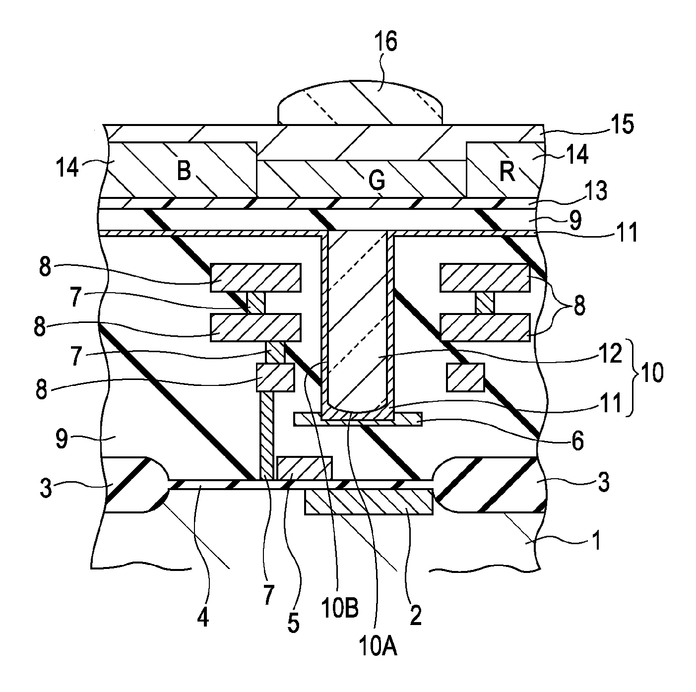
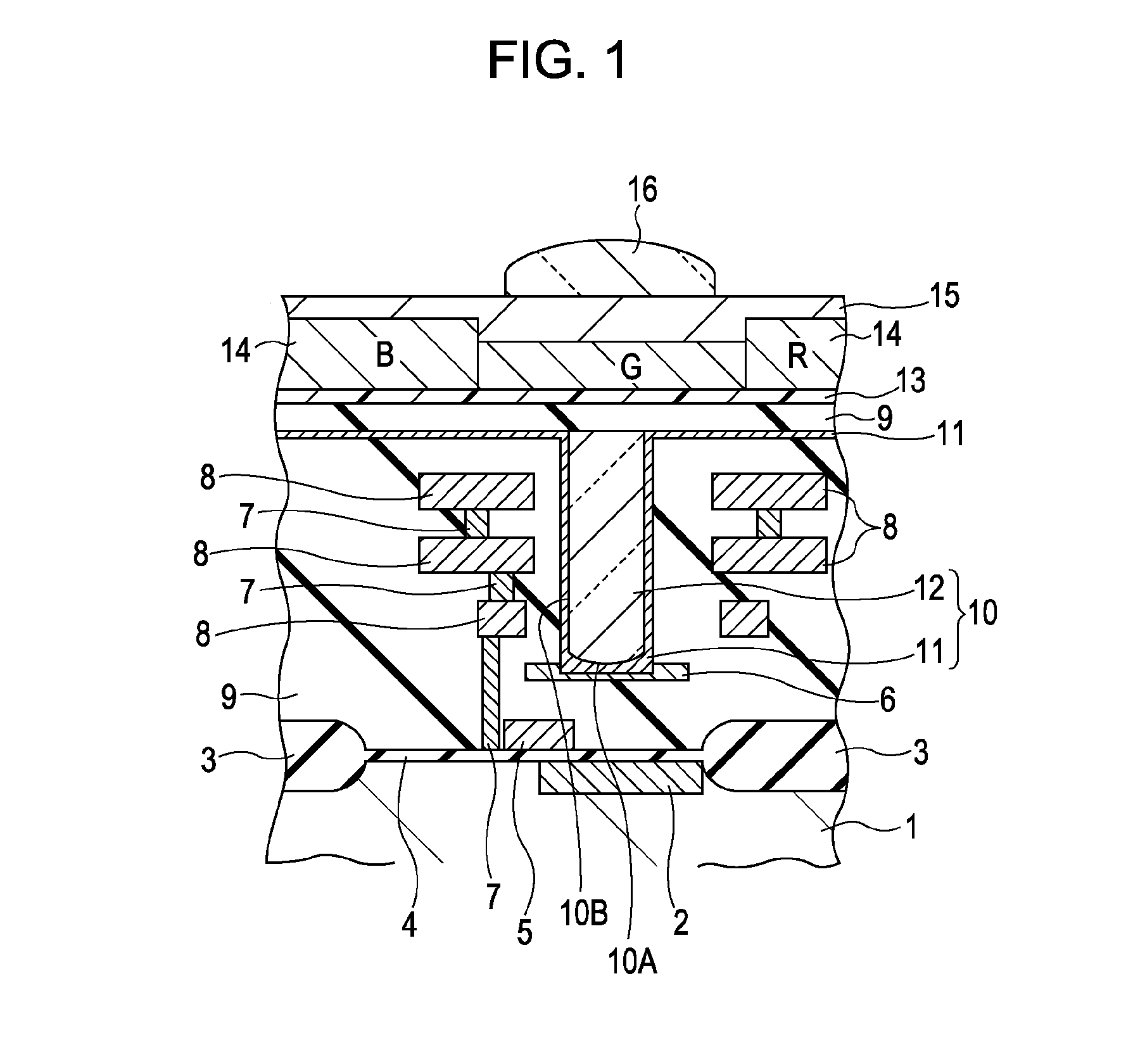
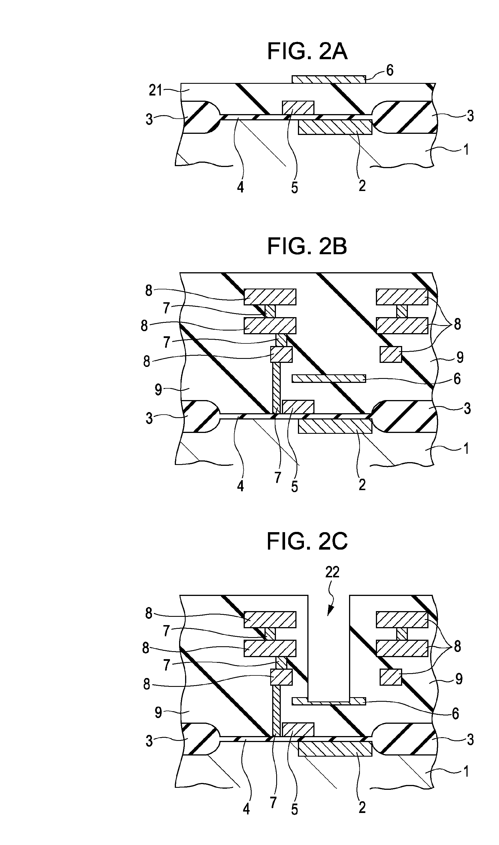
[0035]A waveguide including a cladding and a core is formed above a light receiving unit (photodiode) formed in a semiconductor substrate of a solid-state imaging device. An inner lens having a convex lens surface at the light receiving unit side (lower side) is formed. The inner lens is integrated with the bottom of the waveguide. The cladding of the waveguide includes an insulating layer and a film coating the inner wall of a hole formed in the insulating layer above the light receiving unit. Due to the surface tension that occurs during coating, a curved surface which forms a lens surface of the inner lens can be easily formed at the bottom of the waveguide.

[0036]In forming the cladding of the waveguide, a film that constitutes the cla...


PUM


Abstract

A solid-state imaging device includes a light receiving unit formed in a semiconductor base and configured to perform photoelectric conversion; an insulating layer disposed on the semiconductor base; a film constituting a cladding of a waveguide together with the insulating layer and being formed in an outer part of an interior of a hole by coating, the hole being formed in the insulating layer above the light receiving unit; a core of the waveguide, the core being composed of a material having a higher refractive index than a material for the insulating layer and a material for the film formed by coating, the core being formed in an inner part of the interior of the hole; and an inner lens integrated with the waveguide, the inner lens having a lens surface formed at the bottom of the hole at the interface between the film formed by coating and the core.

Description

BACKGROUND OF THE INVENTION[0001]1. Field of the Invention[0002]The present invention relates to a solid-state imaging device and a method for making the same, and an imaging apparatus including the solid-state imaging device.[0003]2. Description of the Related Art[0004]Heretofore, various proposals have been made on improvements of sensitivity of solid-state imaging devices. One of such proposals is a waveguide structure in which a hole formed directly above a light receiving unit is filled with a high-refractive-index material (refer to Japanese Unexamined Patent Application Publication Nos. 11-121725, 10-326885, and 2005-294749).[0005]FIG. 5 is a schematic diagram of an example of a solid-state imaging device including a waveguide structure. A light receiving unit (photodiode) 52 is formed in a region isolated by a device isolation layer 53 of a semiconductor substrate 51 such as a silicon substrate. A transfer gate electrode 55 is formed on a gate insulating film 54 on the semic...

Claims


Application Information

Patent Timeline
Patent Type & Authority Patents(United States)
IPC IPC(8): H01L31/0232H01L27/14H04N5/335H04N5/369
CPCH01L27/14632H01L27/14629H01L27/14603H01L27/14621H01L27/14627
Inventor MATSUGAI, HIROYASU
Owner SONY SEMICON SOLUTIONS CORP
Why Eureka
Try Eureka