Sensor having improved thermal stability

a technology of thermal stability and sensors, applied in the field of sensors, can solve the problems of increasing power consumption, sensor reliability going worse, and sensor itself malfunctioning, and achieve the effect of reducing the cost of fabrication involved

Inactive Publication Date: 2013-03-05
DAI NIPPON PRINTING CO LTD
View PDF16 Cites 10 Cited by
  • Summary
  • Abstract
  • Description
  • Claims
  • Application Information

AI Technical Summary

Benefits of technology

[0009]With such an inventive sensor wherein the metal wiring is located at and connected onto the insulating layer positioned at the bend of the piezoelectric-resistor, it is possible to keep Joule heat from being generated at the bend of the piezoelectric-resistor, and effectively release off Joule heat generated at the piezoelectric-resistor covered with the insulating layer. It is thus possible to prevent temporal fluctuations of the output values of the sensor, and achieve high-sensitivity sensor function in a stable way. When the diffusion resistance layer is located at the piezoelectric-resistor just below the contact holes, on the other hand, it is possible to reduce the contact resistance of the piezoelectric-resistor with the metal wiring or bridge circuit wiring, thereby holding back the generation of Joule heat.
[0012]In such an inventive sensor fabrication process, it is the first, the second and the third step that are needed for the formation of the piezoelectric-resistors, and at the third step in particular, the metal wiring and the bridge circuit wiring can simultaneously be formed. In other words, the conventional step of diffusing high concentrations of impurities into a silicon substrate for the formation of a high-concentration diffusion layer may be dispensed with. It is thus possible to slash the fabrication costs involved and fabricate a high-performance sensor in a stable way.

Problems solved by technology

However, a problem with this is that only with the use of the short piezoelectric-resistor, there are increasing power consumptions, because voltage is applied to the piezoelectric-resistor during driving.
This in turn triggers off a temporal change in the output value of the sensor, offering a problem that the sensor's reliability goes worse.
Another problem is that wirings for electrically connecting multiple piezoelectric-resistors in series lie on the high-concentration diffusion layer alone, and as defects occur at this side, it directly means malfunction of the sensor itself.

Method used


Image

  • Sensor having improved thermal stability
  • Sensor having improved thermal stability
  • Sensor having improved thermal stability

Examples


Embodiment Construction

[0029]Some embodiments of the invention are now explained with reference to the accompanying drawings.

[Sensor]

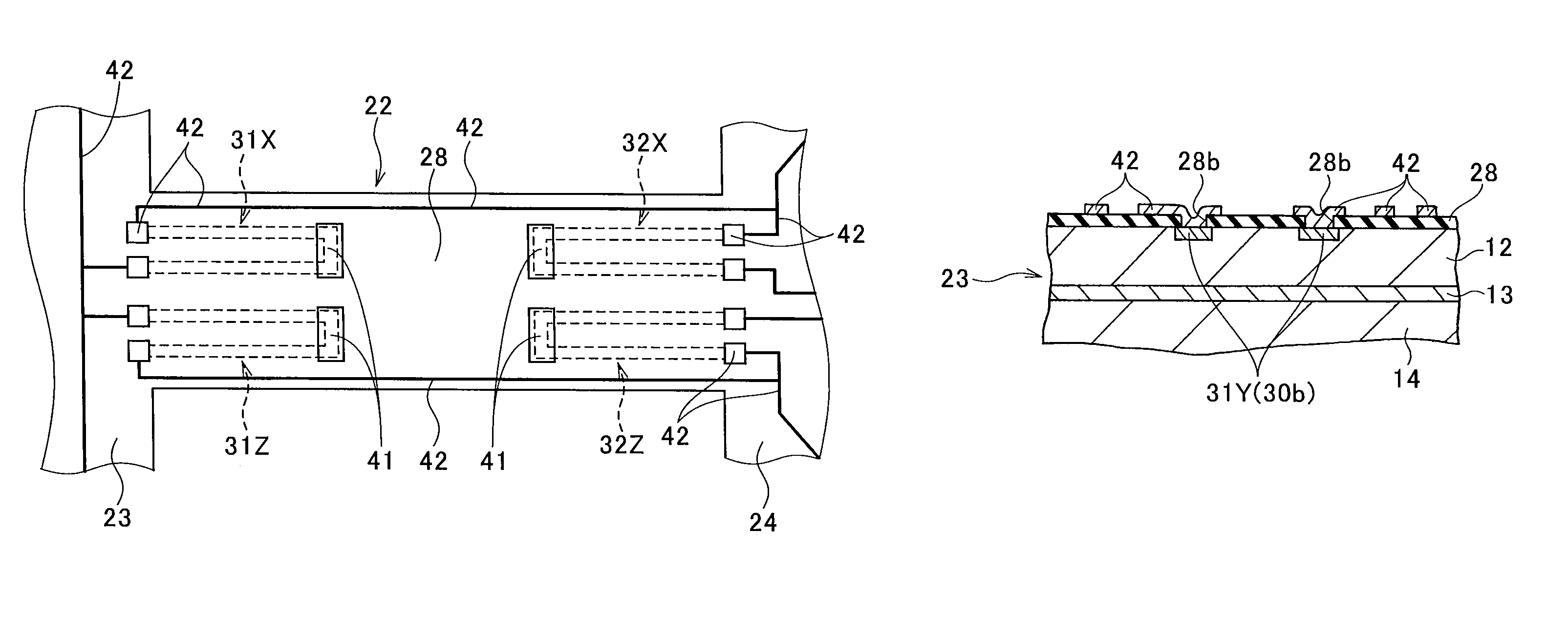
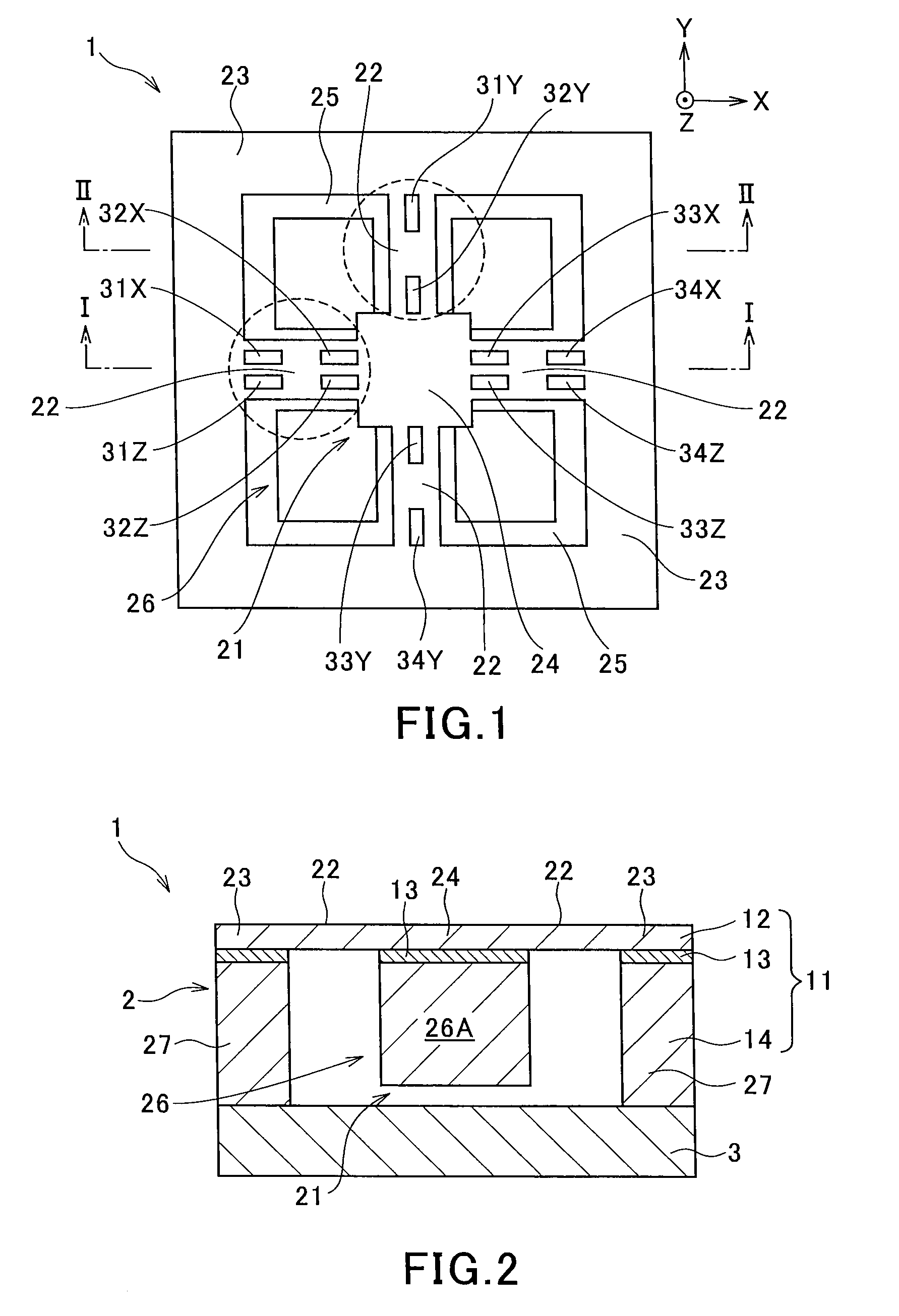
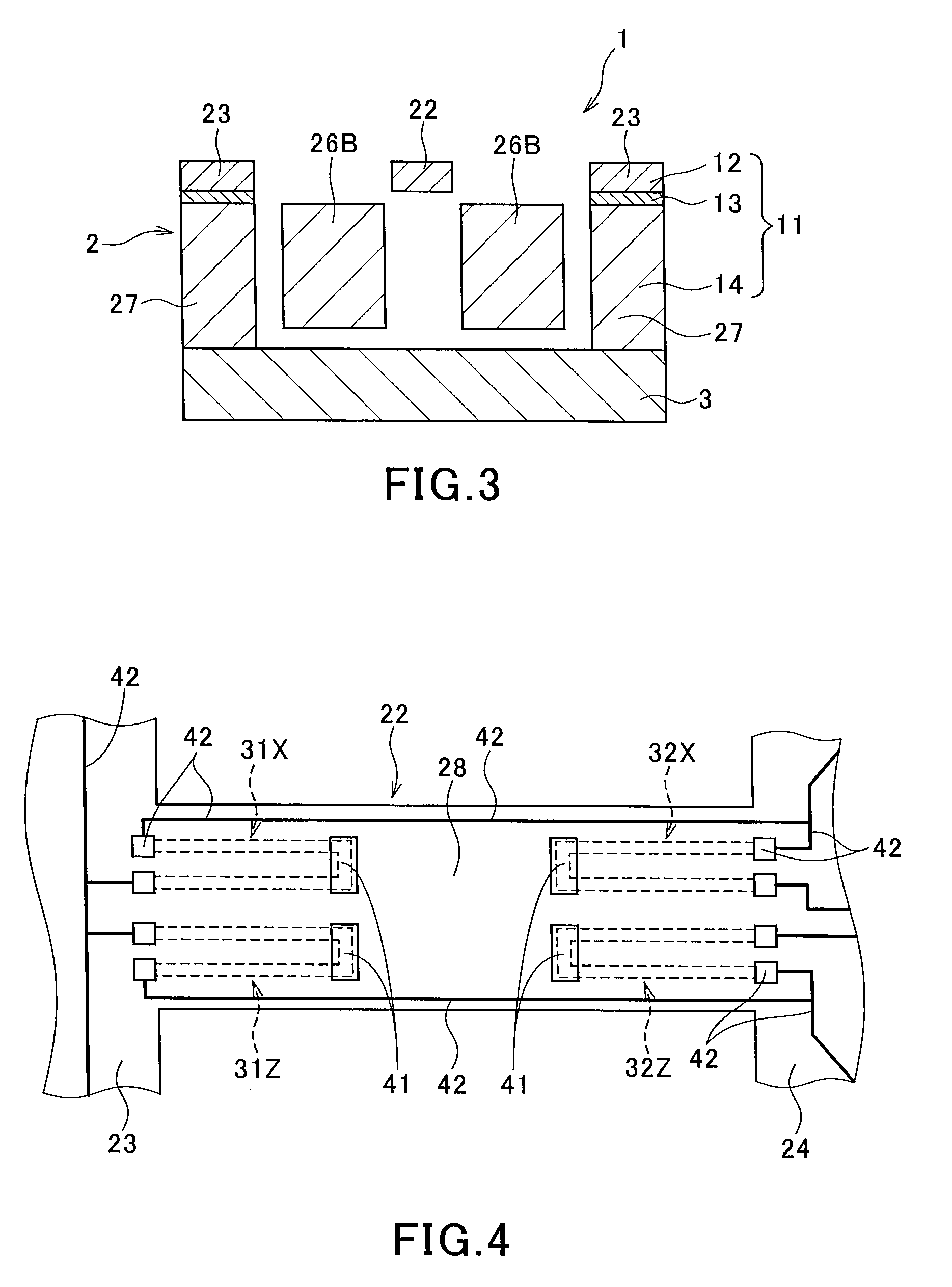
[0030]FIG. 1 is a plan view of an acceleration sensor that is one embodiment of the inventive sensor; FIG. 2 is a sectional view of the sensor of FIG. 1 as taken on line I-I; and FIG. 3 is a sectional view of the sensor of FIG. 1 as taken on line II-II. Referring to FIGS. 1, 2 and 3, a sensor shown generally at 1 comprises a sensor body 2 and a support substrate 3 bonded to the sensor body 2. The sensor body 2 comprises an SOI (silicon on insulator) substrate 11 having a triple-layer structure wherein a silicon oxide layer 13 is sandwiched between a silicon layer 12 (active layer silicon) and a silicon layer 14 (substrate silicon).

[0031]The silicon layer 12 (active layer silicon) forming a part of the sensor body 2 comprises a weight joint 24 forming a weight portion 21, four beams 22 for supporting the weight joint 24, a frame 23 and four windows 25 surrounded with each bea...


PUM

PropertyMeasurementUnit
thicknessaaaaaaaaaa
widthaaaaaaaaaa
widthaaaaaaaaaa

Abstract

The invention provides a sensor comprising a frame, a plurality of beams extending inwardly from said frame, a weight portion supported by the beams, a piezoelectric-resistor formed on each beam and an insulating layer that covers the piezoelectric-resistor. The piezoelectric-resistor has at least one bend, and a metal wiring is located on the insulting layer positioned at the bend. The metal wiring is connected to the bend via at least two contact holes formed in the insulating layer. Contact holes are formed in the insulating layer positioned at both ends of the piezoelectric-resistor, and a bridge circuit wiring is connected to the piezoelectric-resistor via the contact holes.

Description

ART FIELD[0001]The present invention relates generally to a sensor for sensing physical quantities such as acceleration and its fabrication process, and more particularly to a sensor that uses a piezoelectric-resistor as a sensor device and its fabrication process.BACKGROUND ART[0002]In recent years, there has been a rapid progress in the development of small-format sensors harnessing the MEMS (micro-electromechanical systems) technology, and sensors adapted to sense physical quantities such as acceleration have been used in various applications inclusive of cellular phones and game machines, with their applications now under study. Such sensors are fabricated using an SOI wafer having a triple-layer structure of, for instance, a silicon layer / silicon oxide layer / silicon layer. A typical sensor comprises a frame having an opening formed in such a way as to hollow out an SOI wafer, a displaceable weight supported on this frame via a plurality of beams and a piezoelectric-resistor loc...

Claims


Application Information

Patent Timeline
Patent Type & Authority Patents(United States)
IPC IPC(8): G01P15/12G01P15/18H01L29/84
CPCB81B3/0081G01P15/0802G01P15/123G01P15/18B81B2201/0235B81B2203/0109Y10T29/42B81B2207/07G01P2015/084
Inventor AIDA, KAZUHIKOHASHIMOTO, KATSUMIMORI, TOSHIAKI
Owner DAI NIPPON PRINTING CO LTD
Why Eureka
Try Eureka