Method for manufacturing a semiconductor device

a manufacturing method and semiconductor technology, applied in the field of semiconductor technology, can solve the problems of high manufacturing cost, poor heat dissipation, and large leakage of planar bulk silicon cmos structure devices, and achieve the effects of reducing manufacturing cost, poor suppression of sce effects, and large leakag

Active Publication Date: 2013-03-05
INST OF MICROELECTRONICS CHINESE ACAD OF SCI
View PDF7 Cites 8 Cited by
  • Summary
  • Abstract
  • Description
  • Claims
  • Application Information

AI Technical Summary

Benefits of technology

[0006]One object of the present invention is to provide a novel method for manufacturing a bulk silicon fin field effect transistor (FinFET). The method is easily incorporated with and highly compatible with the planar CMOS processes.
[0016]According to the above-mentioned technical solutions, the present invention has the following beneficial effects.
[0017]Firstly, the method for manufacturing a semiconductor device according to the present invention can provide a fin field effect transistor on a bulk silicon substrate. The method overcomes self-heating effects and floating body effects in connection with an SOI FinFET device, and it thus reduces the manufacturing cost.
[0019]Thirdly, the method for manufacturing a semiconductor device according to the present invention can be easily implemented with a simple manufacture process, and is easy to be incorporated with and highly compatible with the planar CMOS processes.

Problems solved by technology

Planar bulk silicon CMOS structure devices have encountered serious challenges.
However, there are several drawbacks for an SOI FinFET, such as high manufacturing cost, poor heat dissipation, floating body effects, poor compatibility with the CMOS processes, etc.
However, the conventional Bulk Silicon FinFET devices have several drawbacks as compared with the SOI FinFET devices, for example: short channel effects (SCEs) cannot be suppressed as required; a leakage path may still be formed with the portion of a fin at the bottom of a channel, which results in a large leakage; and the impurity profile cannot be well controlled.

Method used


Image

  • Method for manufacturing a semiconductor device
  • Method for manufacturing a semiconductor device
  • Method for manufacturing a semiconductor device

Examples


Embodiment Construction

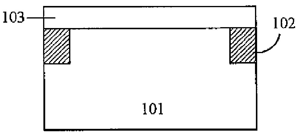
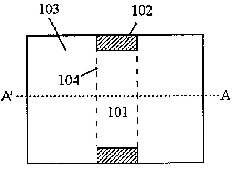
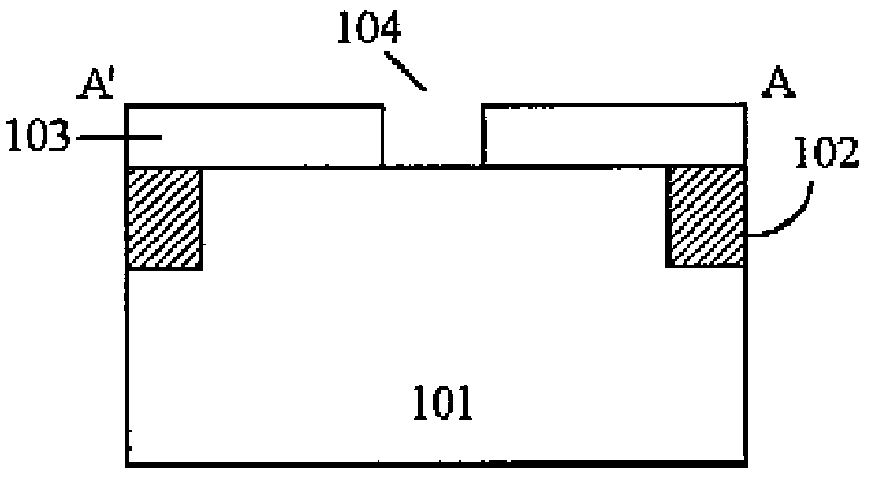
[0032]Hereinafter, the present invention will be described in accordance with a preferred embodiment shown in the attached drawings. However, it should be understood that the description is made for illustration only, rather than limitation to the scope of the present invention. Furthermore, in the following detailed description, the description of well-known structures and technologies are omitted to avoid obscuration of the present invention.

[0033]Schematic diagrams of the layer structure according to an embodiment of the present invention are shown in the attached drawings. These diagrams are not drawn to scale, but some details are exaggerated and other details are omitted for clarity. Shapes, relative sizes and position relationships of various areas and layers are only illustrative. Deviations may be introduced by manufacture tolerance or technical limitations in practice. Furthermore, areas / layers with different shapes, sizes, or relative positions may be designed by one skil...


PUM


Abstract

The present application discloses a method for manufacturing a semiconductor device, comprising: forming a local buried isolation dielectric layer in a semiconductor substrate; forming a fin in the semiconductor substrate and on top of the local buried isolation dielectric layer; forming a gate stack structure on a top surface and side surfaces of the fin; forming source / drain structures in portions of the fin which are on opposite sides of the gate stack structure; and performing metallization. A conventional quasi-planar top-down process is utilized in the present invention to achieve a good compatibility with the CMOS planar processes, easy integration, and suppression of short channel effects, which promotes the development of MOSFETs having reduced sizes.

Description

CROSS-REFERENCE TO RELATED APPLICATION[0001]This application is a National Phase application of, and claims priority to, No. PCT / CN2011 / 072527, filed on Apr. 8, 2011, entitled “METHOD FOR MANUFACTURING A SEMICONDUCTOR DEVICE”, which claims priority to the Chinese Patent Application No. 201110046790.3, filed on Feb. 25, 2011. Both the PCT Application and Chinese Application are incorporated herein by reference in their entireties.FIELD OF THE INVENTION[0002]The present invention relates to semiconductor technology, and in particular, to a method for manufacturing a bulk silicon fin field effect transistor (FinFET).BACKGROUND OF THE INVENTION[0003]With the integrated circuit industry are kept developing according to the Moore Law, feature sizes of CMOS devices are kept shrinking. Planar bulk silicon CMOS structure devices have encountered serious challenges. To solve these issues, various novel device structures have been developed. Among a number of novel device structures, a fin fie...

Claims


Application Information

Patent Timeline
Patent Type & Authority Patents(United States)
IPC IPC(8): H01L21/336
CPCH01L29/66795H01L29/785
Inventor ZHOU, HUAJIEXU, QIUXIA
Owner INST OF MICROELECTRONICS CHINESE ACAD OF SCI
Why Eureka
Try Eureka