Thermal interface material application for integrated circuit cooling

a technology of integrated circuits and thermal interface materials, which is applied in the direction of printed circuit aspects, electrical apparatus construction details, and semiconductor/solid-state device details, etc., can solve the problems of difficult cooling and difficult assembly of individual antennas or antennas on the board, and achieve the effect of improving the thermal interface material application

Active Publication Date: 2013-04-02
GLOBALFOUNDRIES U S INC
View PDF28 Cites 32 Cited by
  • Summary
  • Abstract
  • Description
  • Claims
  • Application Information

AI Technical Summary

Benefits of technology

[0006]Techniques provide improved thermal interface material application in an assembly including an integrated circuit package.
[0013]Advantageously, the above-described techniques provide for improved application of thermal interface material in an integrated circuit package assembly such that the thermal interface material is not degraded or otherwise compromised by other assembly steps. For example, illustrative embodiments of the invention provide efficient cooling paths within an RF module between a cooling device (heat transfer device) and an RFIC. With the inventive fabrication and structural arrangements, the efficiency of heat removal is greatly improved.

Problems solved by technology

However, the assembly of the individual antenna or antennas on the board is problematic in the context of mass production.
However, cooling becomes very challenging since cooling devices used to transfer heat away from the RF module, such as heat sinks and heat spreaders, should be mounted so as not to electromagnetically interfere with the signal transmission / reception of the one or more antennas.

Method used


Image

  • Thermal interface material application for integrated circuit cooling
  • Thermal interface material application for integrated circuit cooling
  • Thermal interface material application for integrated circuit cooling

Examples


Embodiment Construction

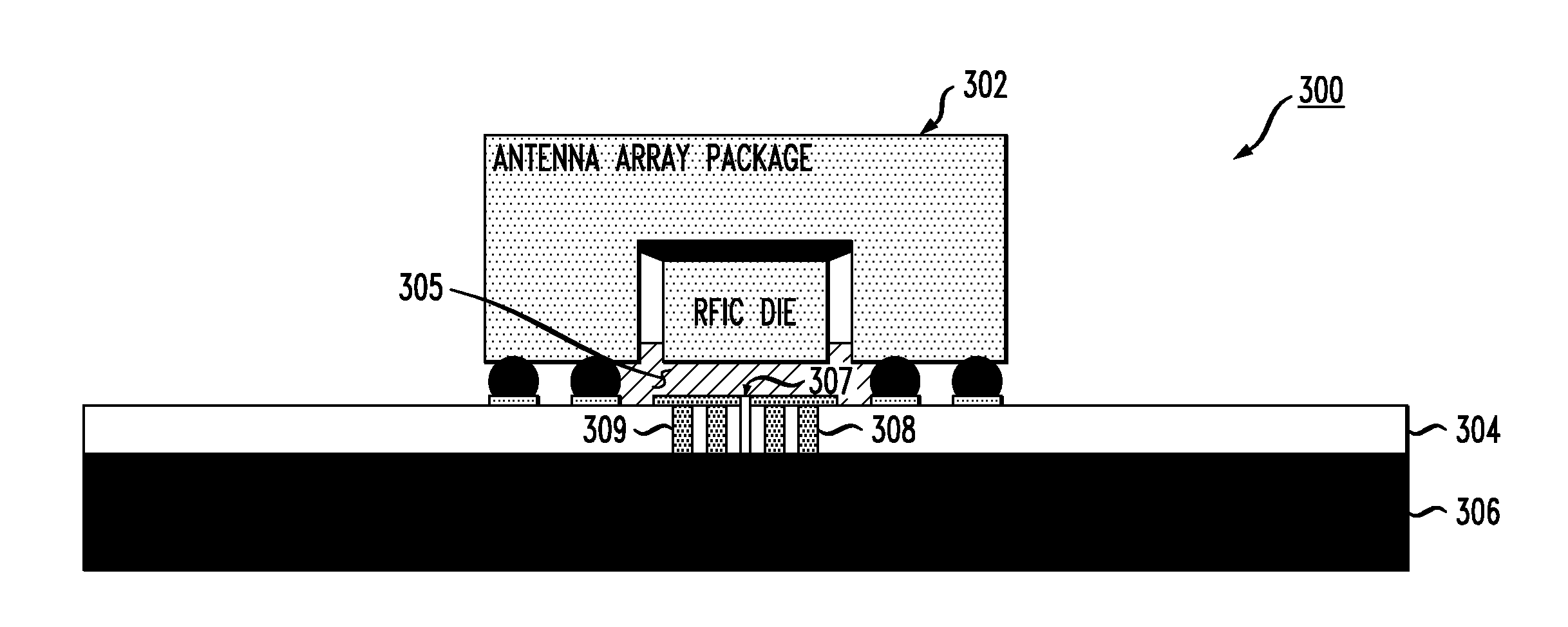
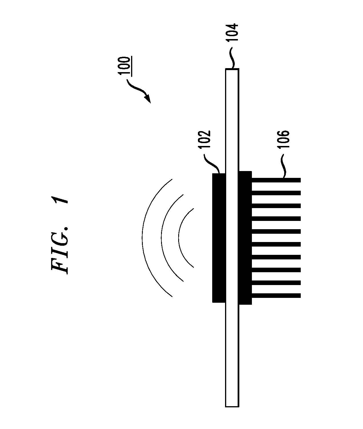
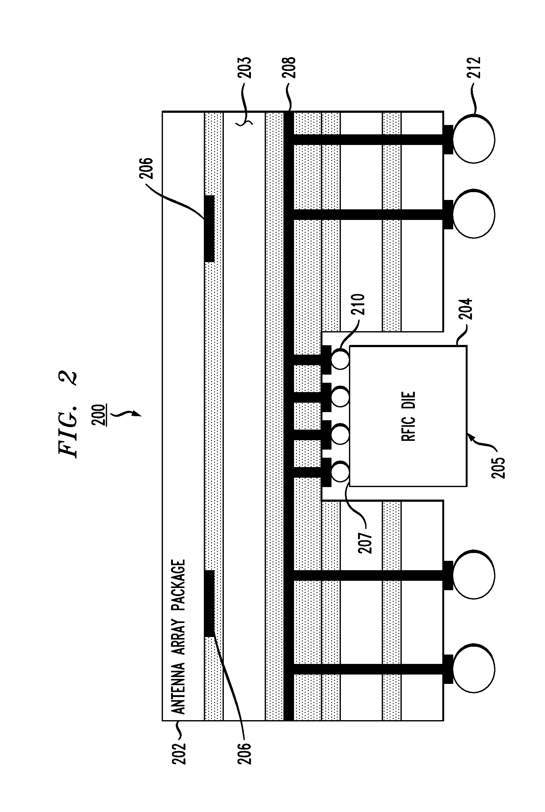
[0019]Principles of the present invention will be described herein in the context of illustrative integrated circuit packages such as a cavity-down type integrated circuit package and illustrative integrated circuit dies such as a radio frequency integrated circuit (RFIC) die. However, it is to be appreciated that the principles of the present invention are not limited to any particular package type or IC die. Rather, the principles of the invention are directed broadly to techniques for improved thermal interface material application in the fabrication process of a printed circuit board assembly that includes an integrated circuit package and a heat transfer device. While principles of the invention are not limited to any particular package or die types, they are well-suited for use in millimeter (mm) wave antenna assemblies.

[0020]As will be illustratively described herein, in the context of various illustrative embodiments, principles of the invention provide techniques that provi...


PUM

PropertyMeasurementUnit
organicaaaaaaaaaa
surface mountingaaaaaaaaaa
thermalaaaaaaaaaa

Abstract

Techniques provide improved thermal interface material application in an assembly associated with an integrated circuit package. For example, an apparatus comprises an integrated circuit module, a printed circuit board, and a heat transfer device. The integrated circuit module is mounted on a first surface of the printed circuit board. The printed circuit board has at least one thermal interface material application via formed therein in alignment with the integrated circuit module. The heat transfer device is mounted on a second surface of the printed circuit board and is thermally coupled to the integrated circuit module. The second surface of the printed circuit board is opposite to the first surface of the printed circuit board.

Description

FIELD OF THE INVENTION[0001]The present invention relates generally to integrated circuit package cooling and, more particularly, to techniques for providing improved thermal interface material application in an assembly including an integrated circuit package.BACKGROUND OF THE INVENTION[0002]In today's portable electronic devices, there are typically one or more radio frequency (RF) modules that serve to provide wireless data exchange between the device and its operating environment. Such an RF module requires one or more antennas to transmit / receive data signals. The RF module and antennas are mounted in some manner on a printed circuit board (PCB).[0003]Until recently, the one or more antennas have been designed independently as a printed shape on the (PCB) or as an individual component to be assembled near an RF integrated circuit (RFIC) die. However, the assembly of the individual antenna or antennas on the board is problematic in the context of mass production.[0004]Recently, ...

Claims


Application Information

Patent Timeline
Patent Type & Authority Patents(United States)
IPC IPC(8): H05K7/20H05K9/00
CPCH05K1/0206H05K3/30Y10T29/49137H05K1/183H05K3/0061H05K2201/10098H05K2201/10477H01L2223/6677H01L2224/131H01L2224/16225H01L2224/73253H01L2924/15153H01L2924/15321H05K1/141Y10T29/49128H01L2924/014
Inventor GAYNES, MICHAEL ANTHONYKAM, DONG GUNLIU, DUIXIANREYNOLDS, SCOTT KEVIN
Owner GLOBALFOUNDRIES U S INC
Why Eureka
Try Eureka