Miniaturized, low power, wireless transmitter and receiver with on-chip antenna, and wireless coupling of on-chip and off-chip antenna

a technology of on-chip antennas and wireless transmitters, applied in the direction of antennas, bulk negative resistance effect devices, transmission, etc., can solve the problems of increasing cost and overall power consumption, low q passives, and low noise of on-chip antennas, so as to achieve 5 mw of power or less, excellent sensitivity, and low resistivity

Active Publication Date: 2013-04-02
KING ABDULLAH UNIV OF SCI & TECH
View PDF8 Cites 12 Cited by
  • Summary
  • Abstract
  • Description
  • Claims
  • Application Information

AI Technical Summary

Benefits of technology

[0020]Preferably, the oscillator TX comprises a VCO and more particularly, is a direct feed open loop VCO TX, and the dual mode active antenna is optimized as both an antenna, and the oscillator inductor. An oscillator TX is a simple architecture, is low power, may be used for short range without a power amplifier, and the oscillator drives the antenna directly. The control line of oscillator is directly modulated by an input signal.
[0032]While the embodiments were designed for the 5 GHz U-NII band, similar design principles may be used to design miniaturized RF RX and RF TX circuits with integrated antennas for operation at other frequencies, e.g. ˜1 GHz to ˜10 GHz. Although standard CMOS implementations provide for low cost fabrication, custom processes or hybrid technologies may be preferred for some applications to optimize performance.

Problems solved by technology

Integration of analog, digital and RF electronics for such applications presents a number of challenges.
On the other hand, substrate noise and low Q passives remain a challenge for efficient CMOS SoC implementations (see for example: A. Natarajan, A. Komijani, X. Guan, A. Babakhani, A. Hajimiri, “A 77-GHz Phased-Array Transceiver With On-Chip Antennas in Silicon: Transmitter and Local LO-Path Phase Shifting,” Solid-State Circuits, IEEE Journal of, vol.
While SoC is a more size efficient approach, on-chip antennas are usually very inefficient when implemented in silicon technology because of the lossy nature of low resistivity silicon substrates.
This approach not only requires a number of design steps, and increases cost and overall power consumption, but the presence of bond wires also makes the module less attractive.
However, this only eliminates the physical connection between the feed line and the antenna; the connections and components required between the integrated circuit (IC) and the antenna feed line cannot be removed.
However, the latter approach has not been demonstrated in chip-to-package coupling.
Also, regardless of frequency band, lossy substrates, parasitic coupling and interference from on-chip circuitry, or, e.g. conductive layers such as interconnect, or metal components such as batteries, in the vicinity of an antenna, can affect the design and performance.
Modeling and simulations that take into account these effects, and characterization of on-chip antennas by measurement of actual antenna gain and radiation pattern is complex.
Antenna performance may be adversely affected by parasitic coupling and by interference between the antenna and the circuitry surrounding the on-chip antenna.
Thus, although circuits with on-chip antennas have been demonstrated, actual performance of most of these antennas has not been characterized, and in practice, on-chip antennas are not usually implemented because of the above-mentioned problems with lossy substrates, interference issues and characterization challenges.

Method used


Image

  • Miniaturized, low power, wireless transmitter and receiver with on-chip antenna, and wireless coupling of on-chip and off-chip antenna
  • Miniaturized, low power, wireless transmitter and receiver with on-chip antenna, and wireless coupling of on-chip and off-chip antenna
  • Miniaturized, low power, wireless transmitter and receiver with on-chip antenna, and wireless coupling of on-chip and off-chip antenna

Examples


first embodiment

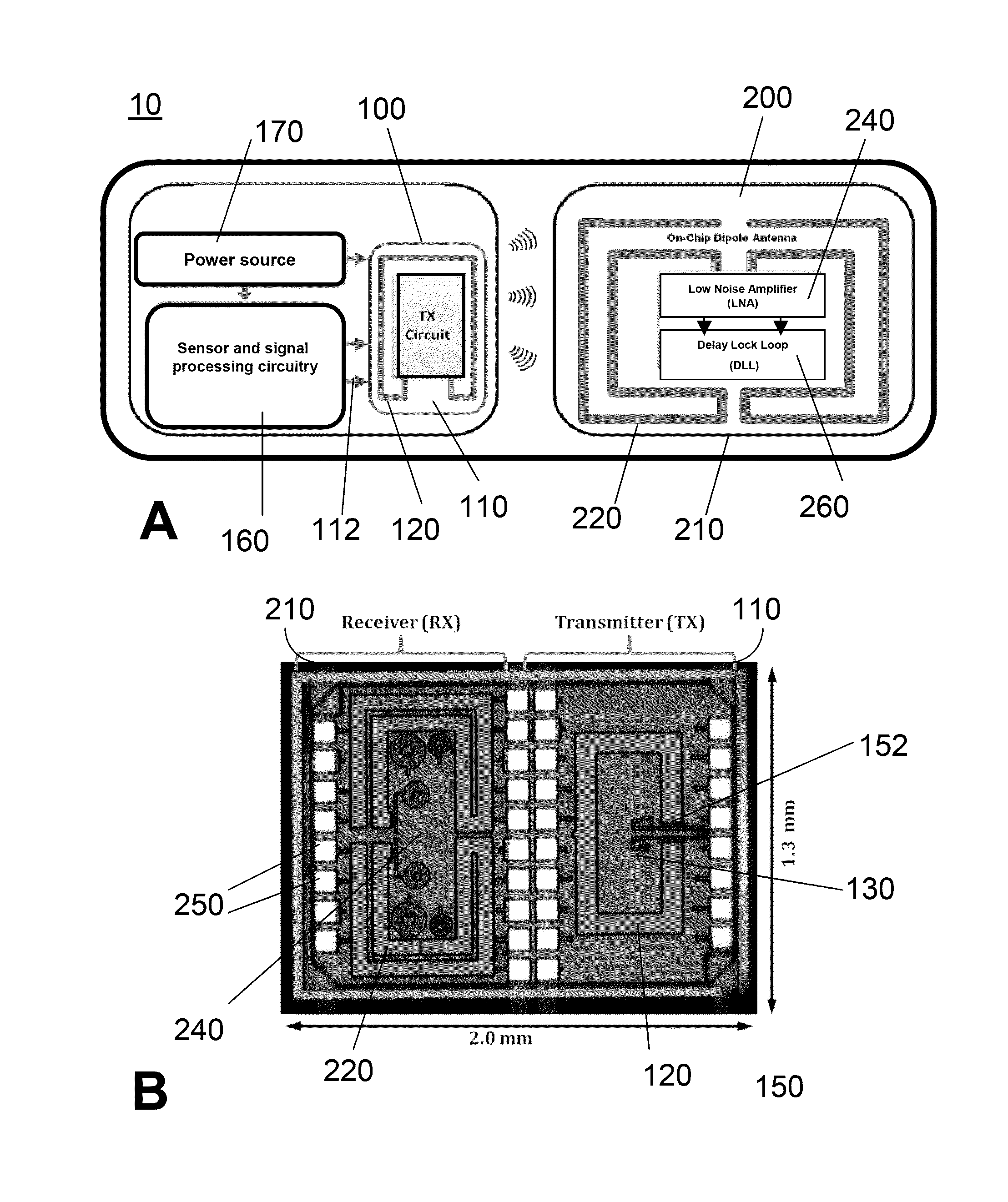
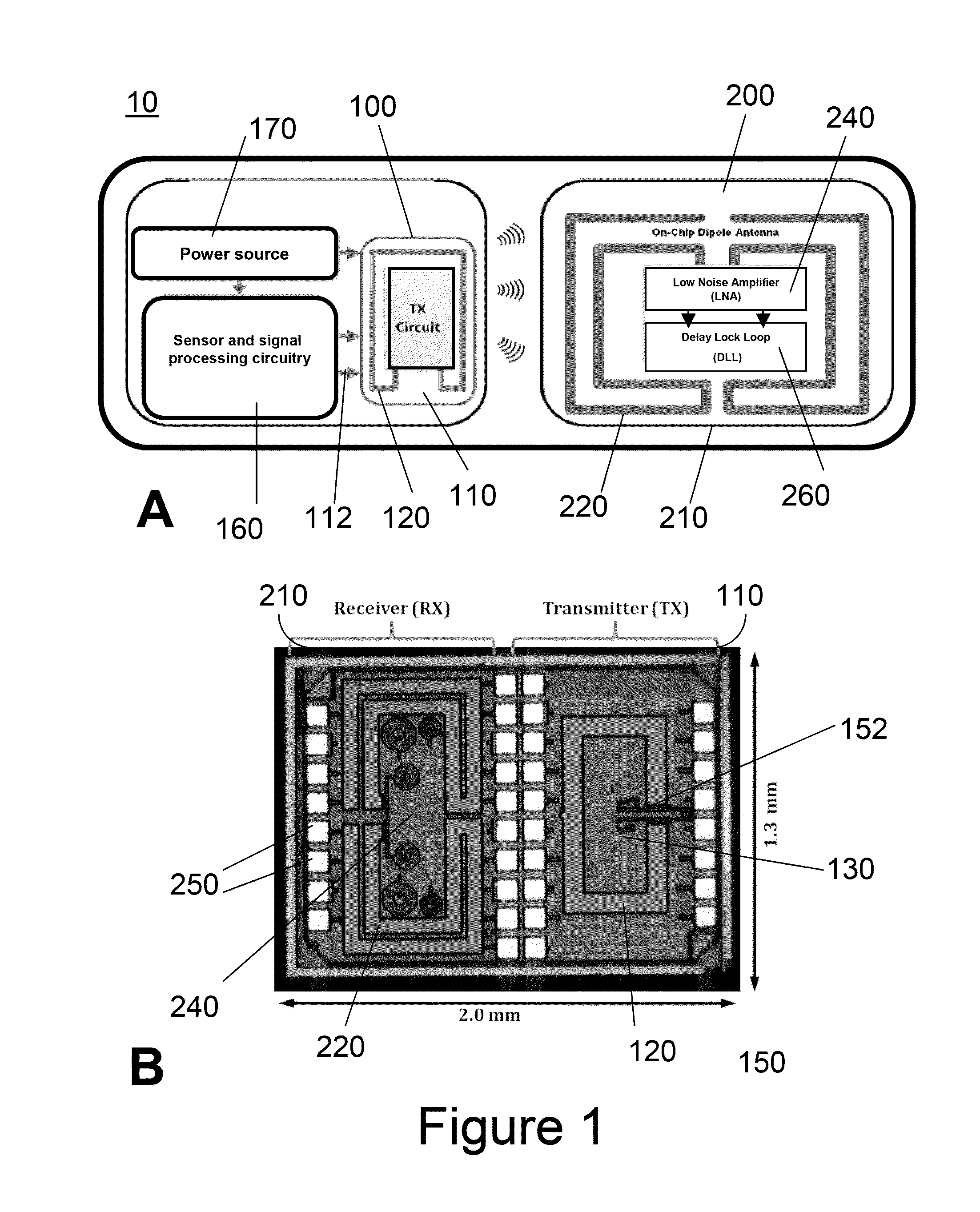
[0069]As illustrated in FIG. 1A, a transmitter / receiver system 10 according to the present invention comprises a CMOS integrated circuit which comprises a monolithically integrated circuit (transmitter chip) 100 comprising a transmitter 110, and a monolithically integrated circuit (receiver chip) 200 comprising a receiver 210. In this exemplary embodiment, the transmitter 100 comprises a data signal source 160, which may be on a separate chip or monolithically integrated with the transmitter 110. The signal source 160 comprises, by way of example only, a low voltage sensor such as a biomedical sensor, integrated with signal processing electronics, and provided on a separate substrate. The data signal source generates a suitable low voltage output, which directly feeds the input 112 of the oscillator transmitter circuit 110. The oscillator transmitter circuit 110 comprises an on-chip loop antenna 120, as will be described in detail below (page 14). Also shown in FIG. 1A is an on-chip...

second embodiment

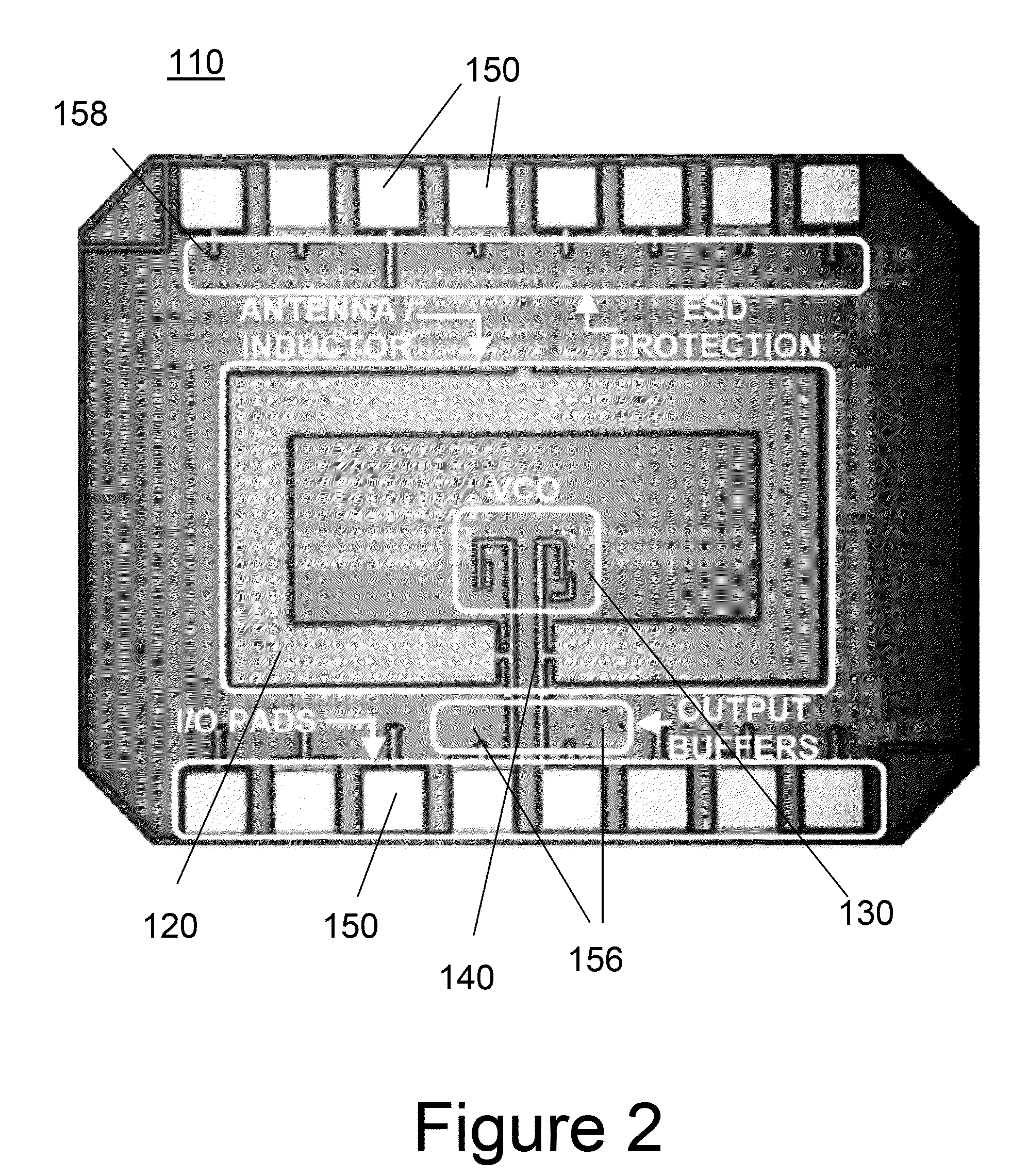
[0087]A photomicrograph of a monolithically integrated RF transmitter circuit 300 according to the present invention comprises an on-chip folded dipole antenna 320 is shown in FIG. 7. The RF RX circuit 300 comprises an on-chip antenna 320 monolithically integrated with a differential LNA 340 and DLL demodulator 360, which may be realized in a standard 0.13 μm CMOS process technology on a low resistivity 13.5 Ω-cm silicon substrate. FIG. 8 shows a schematic of the antenna geometry used for simulations and placement of the LNA and DLL demodulator within the area defined by the folded dipole antenna. The front end of the receiver is a low power, high gain LNA that is conjugately matched to an on-chip antenna, and designed to reject noise and improve received signal strength. The impedances of the on-chip antenna 320 and differential LNA are conjugately matched over a wide frequency range through the co-design of the circuits and antenna for simultaneous low noise and input power matchi...


PUM


Abstract

A miniaturized, low power RF transmitter with a dual mode active on-chip antenna / inductor is disclosed in which antenna also serves as the oscillator inductor. Also disclosed is a miniaturized low power RF receiver with an on-chip antenna; and a RF transmitter system wherein an on-chip antenna is wirelessly coupled to an off chip patch antenna are disclosed. Advantageously, the TX chip is housed in a low loss, e.g. Low Temperature Co-fired Ceramic (LTCC) package with a patch antenna to provide a System-on-Package implementation comprising electromagnetic coupling between a RF TX chip comprising an integrated on-chip antenna and a package antenna. The on-chip antenna feeds the LTCC patch antenna through aperture coupling, thus negating the need for RF buffer amplifiers, matching elements, baluns, bond wires and package transmission lines, and significantly increases the gain and range of the module with respect to the on-chip antenna alone, without deterioration of the circuit performance and power consumption. Exemplary embodiments are disclosed which may be fabricated using standard CMOS technology, for operation in the 5 GHz U-NII band for applications such as miniaturized, low cost, low power wireless devices and sensor systems.

Description

CROSS REFERENCE TO RELATED APPLICATIONS[0001]This application claims priority from U.S. provisional application Ser. No. 61 / 105,921, entitled “Miniature Wearable Wireless Biomedical Sensor System”, filed 16 Oct. 2008, which is incorporated herein by reference.FIELD OF THE INVENTION[0002]This invention relates to miniaturized, low power, wireless transmitters and receivers with on-chip antennas, wireless coupling of on-chip and off-chip or package antennas, and more particularly, to system on-chip (SoC) and System-on-Package (SoP solutions for a range of low power wireless communications, such as wireless LAN and sensor systems for biomedical applications.BACKGROUND OF THE INVENTION[0003]The use of mobile, handheld or fixed wireless devices for voice and data communications, monitoring, tracking, controlling, test and measurement has been growing prolifically in recent years as further advances in miniaturized, lower power, low cost electronics are achieved. Wireless terminals and ne...

Claims


Application Information

Patent Timeline
Patent Type & Authority Patents(United States)
IPC IPC(8): H04M1/00
CPCG01T1/026H01L27/14659
Inventor SHAMIM, ATIFARSALAN, MUHAMMADROY, LANGIS
Owner KING ABDULLAH UNIV OF SCI & TECH
Why Eureka
Try Eureka