Lateral insulated gate bipolar transistor (LIGBT)

a bipolar transistor and gate technology, applied in the field of lateral insulated gate bipolar transistors (ligbts), to achieve the effect of suppressing the formation of a schottky barrier,/or the height of the energy barrier, and reducing the width of the depletion region

Inactive Publication Date: 2013-04-09
POWER INTEGRATIONS INC
View PDF1 Cites 2 Cited by
  • Summary
  • Abstract
  • Description
  • Claims
  • Application Information

AI Technical Summary

Problems solved by technology

Furthermore, a lower, substrate region of the IC does not form a part of the active device—the devices are actually isolated from such lower regions of the IC.

Method used


Image

  • Lateral insulated gate bipolar transistor (LIGBT)
  • Lateral insulated gate bipolar transistor (LIGBT)
  • Lateral insulated gate bipolar transistor (LIGBT)

Examples


Embodiment Construction

[0091]The following describes arrangements falling within the broader aspects of the present invention summarised above, and more specific embodiments.

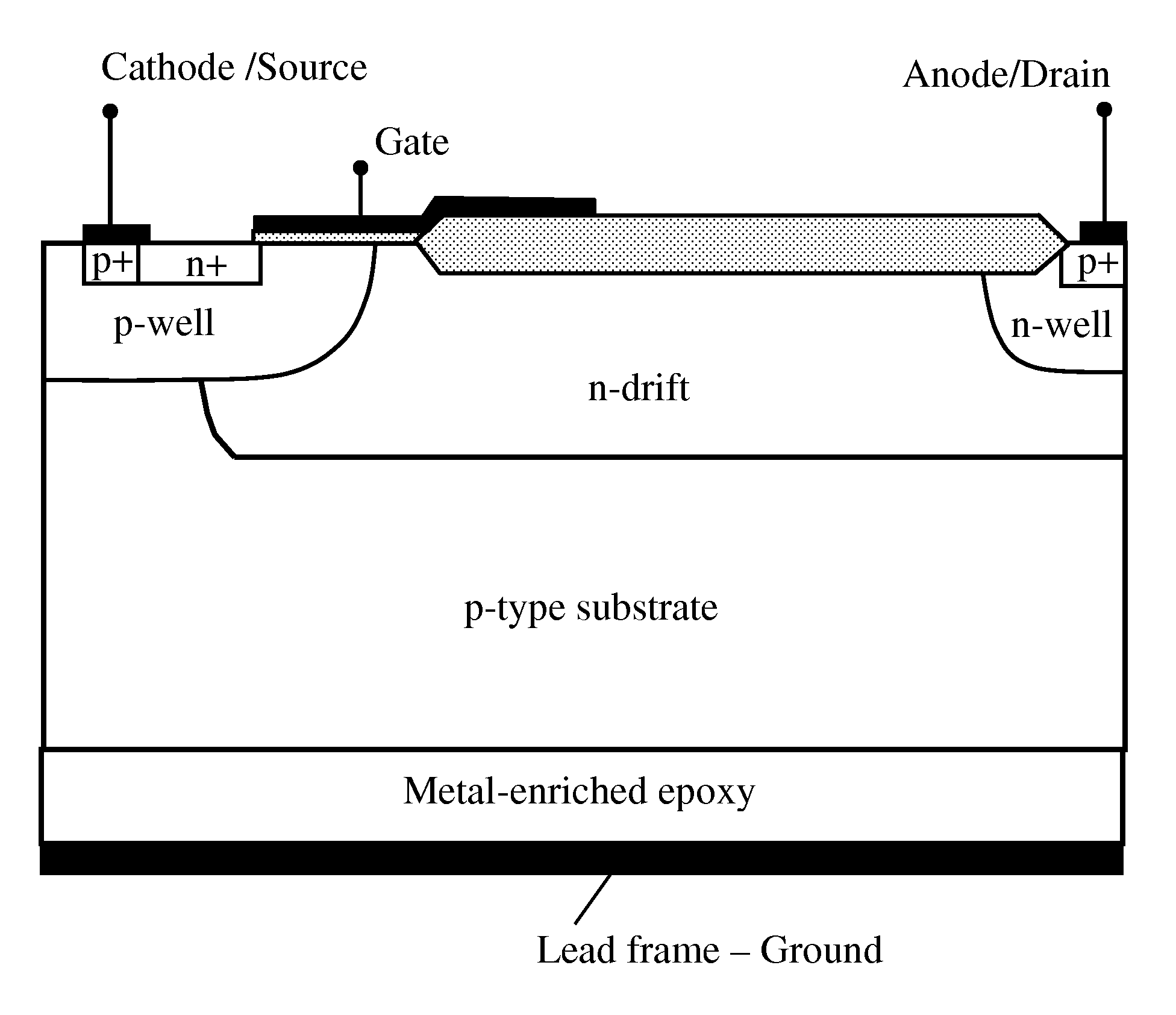
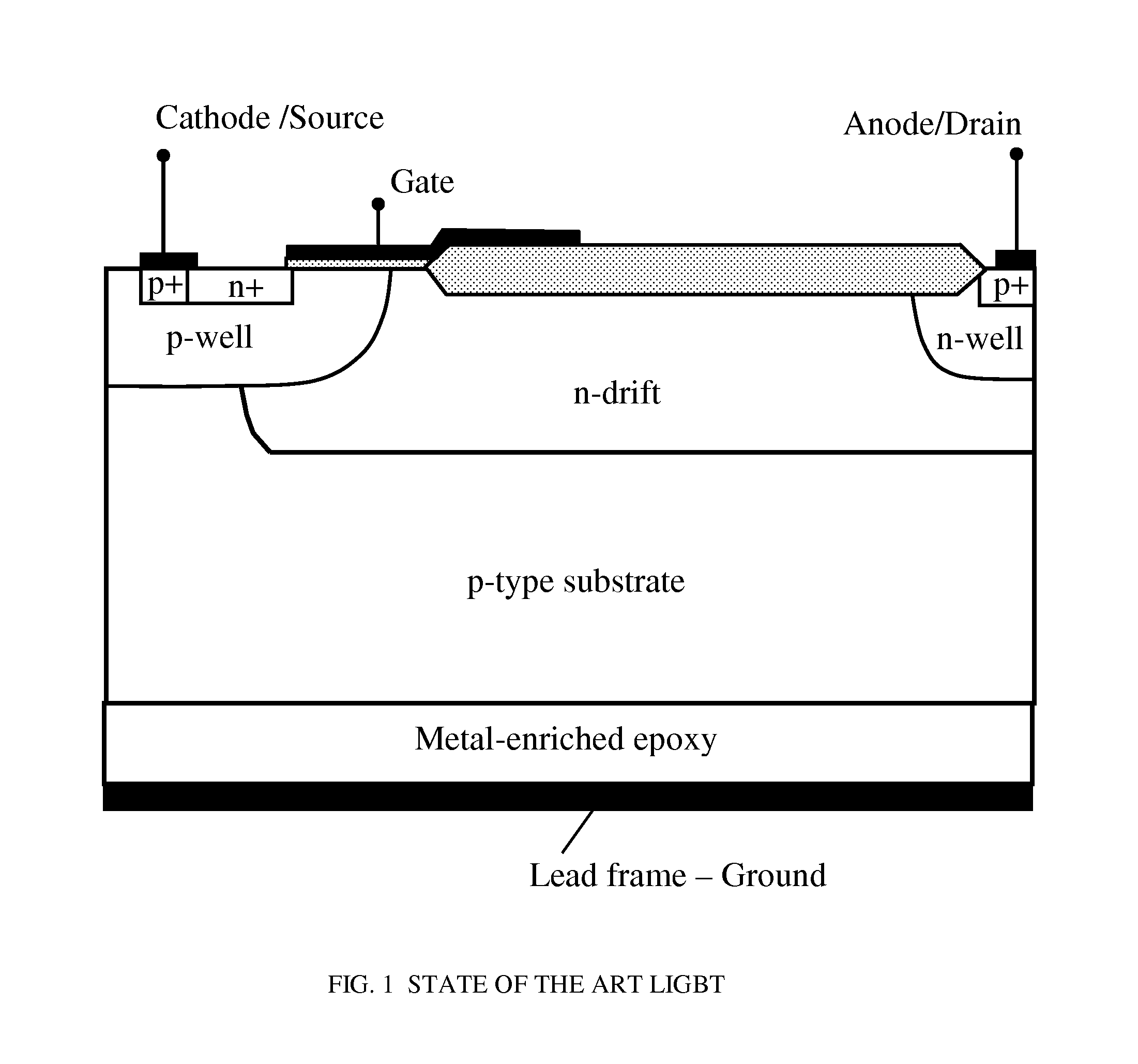
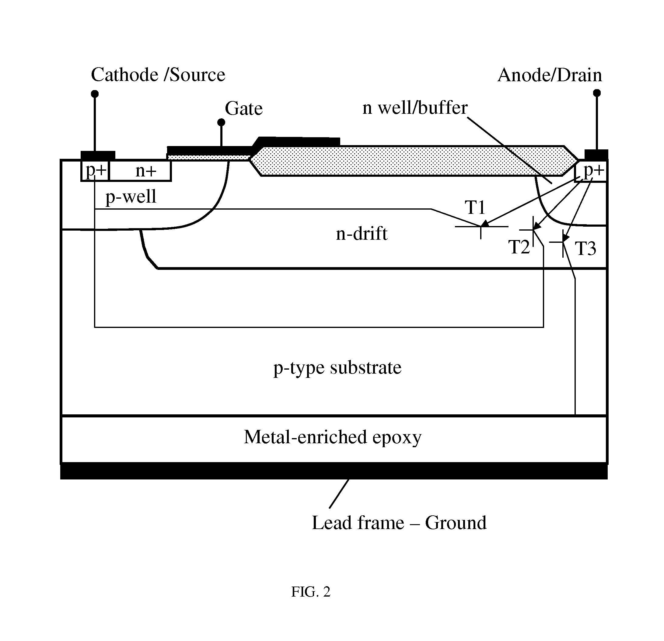
[0092]In an LIGBT device, a rated off-state breakdown of the device may be achieved by appropriate doping levels and dimensions of the drift layer and the substrate region. The presence of a lowly-doped substrate region below the drift region may help to distribute more uniformly the electric field and potential lines within the drift region and hence help to increase the voltage breakdown ability of the device. This is known as the RESURF effect. For an effective RESURF, the substrate region is preferably more lowly-doped than the drift region (e.g., by 5× to 10× times). Nevertheless the presence of an open substrate may have detrimental effects on the switching as plasma is deeply accumulated in the lowly-doped substrate and its removal during turn-off can take a long time and result in high turn-off losses.

[0093]In general, any emb...


PUM


Abstract

This invention generally relates to LIGBTs, ICs comprising an LIGBT and methods of forming an LIGBT, and more particularly to an LIGBT comprising a substrate region of first conductivity type and peak dopant concentration less than about 1×10¹⁷ / cm3; a lateral drift region of a second, opposite conductivity type adjacent the substrate region and electrically coupled to said substrate region; a charge injection region of the first conductivity type to inject charge toward said lateral drift region; a gate to control flow of said charge in said lateral drift region; metal enriched adhesive below said substrate region; and an intermediate layer below said substrate region to substantially suppress charge injection into said substrate region from said metal enriched adhesive.

Description

FIELD OF THE INVENTION[0001]This invention generally relates to Lateral Insulated Gate Bipolar Transistors (LIGBTs), for example in integrated circuits (ICs), and methods of forming an LIGBT.BACKGROUND TO THE INVENTION[0002]Power devices operated in integrated circuits typically operate with a voltage in the range 20V to 1.2 kV and typically higher than 30V or 50V or so. Power devices typically operate with a current in the range 10 mA to 50 A and typically higher than 0.1 A and smaller than 5 A. Such devices may also be referred to as “high voltage / power devices”. These devices are typically capable of delivering from a few mWatts to 1 Watt or even a few tens of Watts of power. Their application may range from domestic appliances, electric cars, motor control, and power supplies to RF and microwave circuits and telecommunication systems.[0003]Lateral devices in integrated circuits have the high voltage / low voltage main terminals (variously called the anode / cathode, drain / source and...

Claims


Application Information

Patent Timeline
Patent Type & Authority Patents(United States)
IPC IPC(8): H01L29/739H01L21/331
CPCH01L29/402H01L29/7394
Inventor UDREA, FLORINPATHIRANA, VASANTHATRAJKOVIC, TANYAUDUGAMPOLA, NISHAD
Owner POWER INTEGRATIONS INC
Why Eureka
Try Eureka