Semiconductor device with improved pixel arrangement

a semiconductor device and pixel arrangement technology, applied in the direction of organic semiconductor devices, discharge tubes/lamp details, discharge tubes luminescnet screens, etc., can solve the problem of the size of a light emitting device, and achieve the effect of reducing the size of the partition, preventing defects, and increasing the number of steps

Active Publication Date: 2013-05-14
SEMICON ENERGY LAB CO LTD
View PDF131 Cites 29 Cited by
  • Summary
  • Abstract
  • Description
  • Claims
  • Application Information

AI Technical Summary

Benefits of technology

[0013]The present invention provides a structure which prevents a defect due to precision, bending, and the like of a mask used at the time of evaporation without increasing the number of steps.
[0014]Demands for higher definition, higher aperture ratio, and higher reliability on a full-color flat panel display using emission colors of red, green, and blue has been increased. Such demands are major issues in advancing miniaturization of each display pixel pitch associated with an improvement in definition (increase in the number of pixels) and a reduction in size of a light emitting device. It is necessary to reduce also the upper surface shape of a partition in order to improve definition of an active matrix light emitting device or a passive matrix light emitting device. The present invention provides a partition which realizes display with higher definition by reducing the upper surface shape and a light emitting device including that partition.

Problems solved by technology

Such demands are major issues in advancing miniaturization of each display pixel pitch associated with an improvement in definition (increase in the number of pixels) and a reduction in size of a light emitting device.

Method used


Image

  • Semiconductor device with improved pixel arrangement
  • Semiconductor device with improved pixel arrangement
  • Semiconductor device with improved pixel arrangement

Examples


embodiment mode 1

(Embodiment Mode 1)

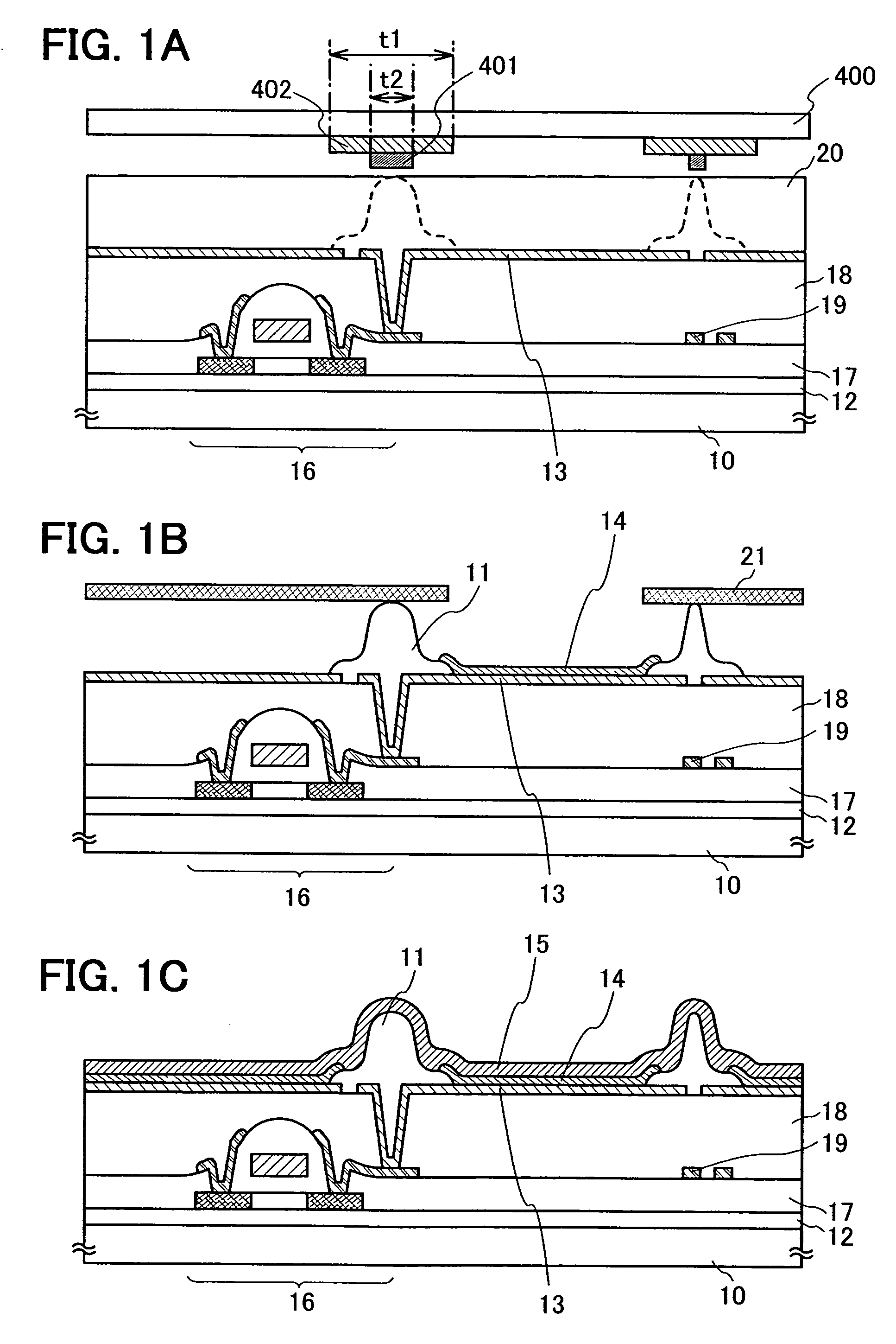
[0054]Here, the present invention is explained using an example of an active matrix light emitting device.

[0055]In addition, an example of a manufacturing process for obtaining a structure of FIG. 1C is hereinafter described.

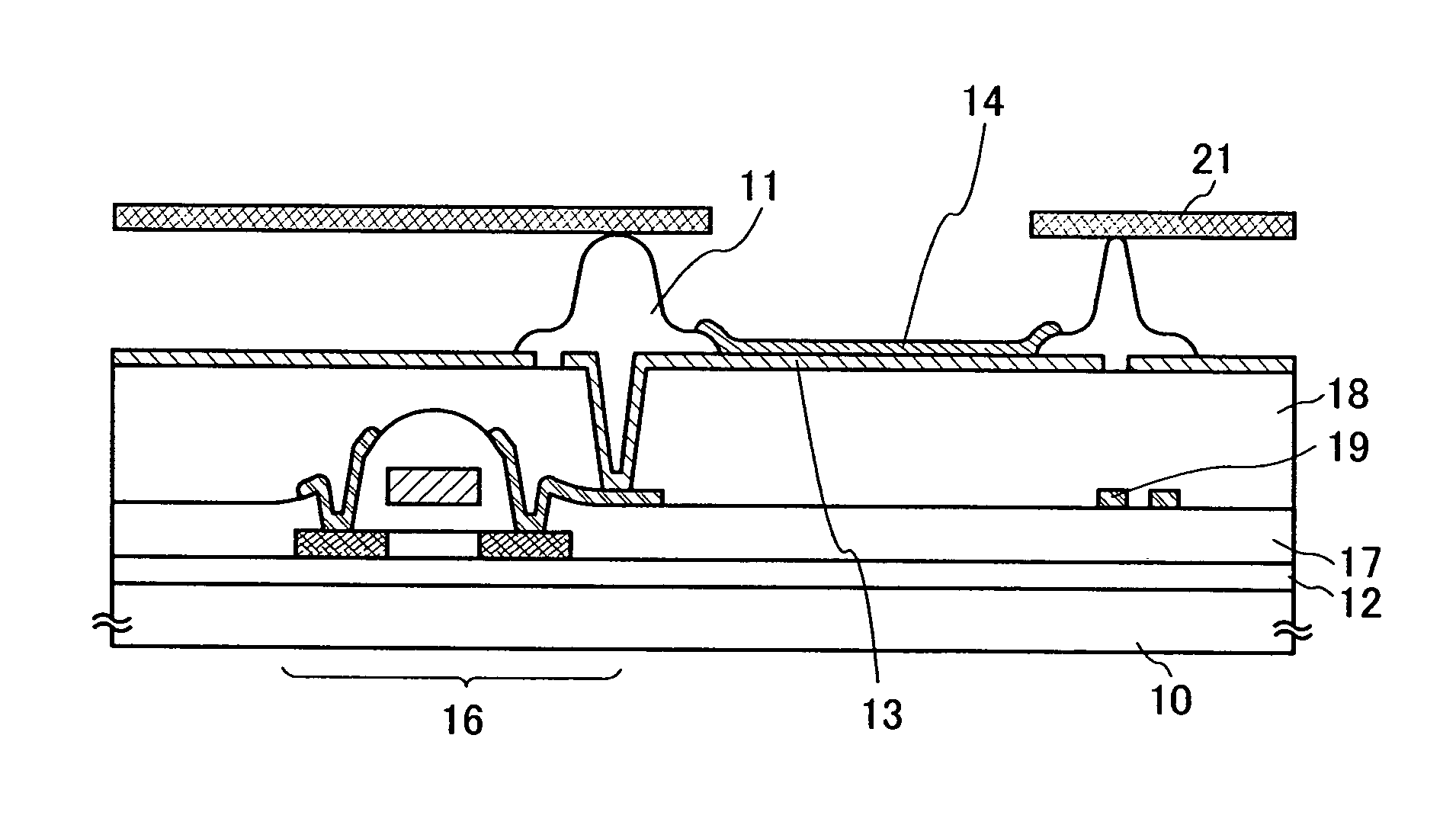
[0056]First, a TFT 16 is manufactured over a substrate 10 having an insulating surface. As for a base insulating film 12 of the TFT 16 and a stacked layer 17 of insulating films including a gate insulating film, an inorganic material (such as silicon oxide, silicon nitride, silicon oxynitride, a SiOF film, or a SiONF film) obtained by a sputtering method or a PCVD method is used. As for an insulating film 18 functioning as an interlayer insulating film, an inorganic material (such as silicon oxide, silicon nitride, silicon oxynitride, a SiOF film, or a SiONF film) obtained by a sputtering method, a PCVD method, or a coating method; a photosensitive or non-photosensitive organic material (such as polyimide, acrylic, polyamide, polyimide amide, ...

embodiment mode 2

(Embodiment Mode 2)

[0080]This embodiment mode describes an example of a structure which is partially different from that of Embodiment Mode 1 with reference to FIG. 3.

[0081]Here, a structure in which one layer of the interlayer insulating film in FIGS. 1A to 1C is reduced, specifically, a structure in which the insulating film 18 shown in FIGS. 1A to 1C is not formed is described. Note that in FIG. 3, the same reference numeral is used to denote the same portion as that in FIGS. 1A to 1C.

[0082]Similarly to Embodiment Mode 1, a TFT 16 is manufactured over a substrate 10 having an insulating surface. Next, a first electrode 33 serving as an anode is formed over a stacked layer 17 of insulating films including a gate insulating film. The first electrode 33 is formed over the stacked layer 17 of insulating films including a gate insulating film so as to be partially in contact with and overlapped with an electrode electrically connected to a source region or a drain region of the TFT.

[0...

embodiment mode 3

(Embodiment Mode 3)

[0089]This embodiment mode describes an example of providing a partition in a pixel portion where a plurality of light emitting elements is arranged (also referred to as a display region) and a structure arranged to surround the pixel portion.

[0090]Here, an example of manufacturing a passive matrix light emitting device is described with reference to FIGS. 4A and 4B.

[0091]A first electrode 303 is formed over a first substrate 301, and a partition 302 is formed to cover an end portion of the first electrode 303. In addition, a structure 304 is formed in the same step as the partition 302. The partition 302 and the structure 304 have different thicknesses. A cross-sectional view at this stage is shown in FIG. 4A.

[0092]Next, a layer 305 containing an organic compound is formed over the first electrode 303, and a second electrode 307 is formed thereover. Note that in forming the layer 305 containing an organic compound by an evaporation method, the structure 304 can p...


PUM


Abstract

As a result of miniaturization of a pixel region associated with an improvement in definition and an increase in a substrate size associated with an increase in area, defects due to precision, bending, and the like of a mask used at the time of evaporation have become issues. A partition including portions with different thicknesses over a pixel electrode (also referred to as a first electrode) in a display region and in the vicinity of a pixel electrode layer is formed, without increasing the number of steps, by using a photomask or a reticle provided with an auxiliary pattern having a light intensity reduction function made of a diffraction grating pattern or a semi-transmissive film.

Description

BACKGROUND OF THE INVENTION[0001]1. Field of the Invention[0002]The present invention relates to a light emitting device using a light emitting element which generates fluorescence or phosphorescence by applying an electric field to the element provided with a layer containing an organic compound (hereinafter referred to as an “organic compound layer”) between a pair of electrodes, and a manufacturing method of the light emitting device. Note that the light emitting device refers to an image display device, a light emitting device, and a light source (including a lighting system).[0003]2. Description of the Related Art[0004]A light emitting element using an organic compound as a luminous body, which has features such as thinness, lightness, high-speed response, and DC drive at low voltage, is expected to be applied to a next-generation flat panel display. In particular, a display device in which light emitting elements are arranged in matrix is considered to have an advantage in a w...

Claims


Application Information

Patent Timeline
Patent Type & Authority Patents(United States)
IPC IPC(8): H01L29/04H01L29/06H05B44/00
CPCH01L27/3246H01L27/3258H01L27/3262H01L33/36H01L51/0011H01L2251/5338H10K59/122H10K71/166H01L21/67359H10K71/00H10K50/80H10K59/10H10K59/124H10K59/1213H10K2102/311
Inventor KUWABARA, HIDEAKIOHNUMA, HIDETO
Owner SEMICON ENERGY LAB CO LTD
Why Eureka
Try Eureka