Polysilicon films by HDP-CVD

a technology of polysilicon and cvd, which is applied in the direction of coating, chemical vapor deposition coating, metallic material coating process, etc., can solve the problems of structural features of the device having decreased spatial dimensions and difficulty in filling the gap with material

Inactive Publication Date: 2013-05-28
APPLIED MATERIALS INC
View PDF418 Cites 336 Cited by
  • Summary
  • Abstract
  • Description
  • Claims
  • Application Information

AI Technical Summary

Problems solved by technology

The decreasing feature sizes result in structural features on the device having decreased spatial dimensions.
The widths of gaps and trenches on the device narrow to a point where the aspect ratio of gap depth to its width becomes high enough to make it challenging to fill the gap with material.

Method used


Image

  • Polysilicon films by HDP-CVD
  • Polysilicon films by HDP-CVD
  • Polysilicon films by HDP-CVD

Examples


Embodiment Construction

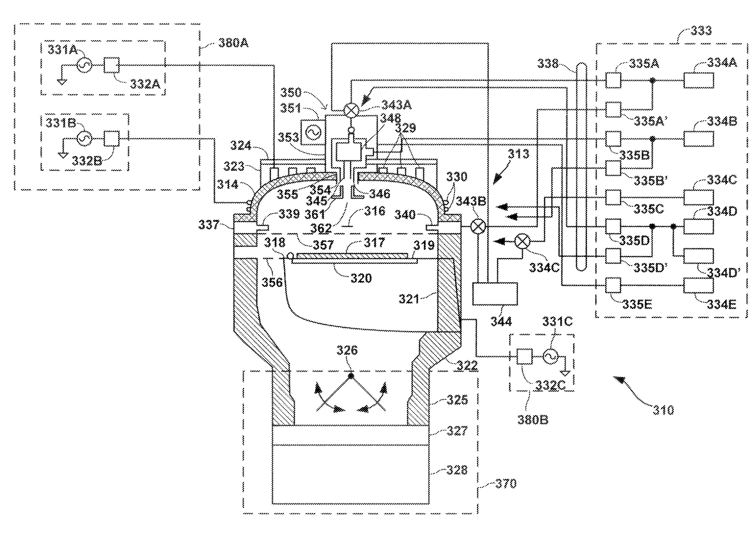
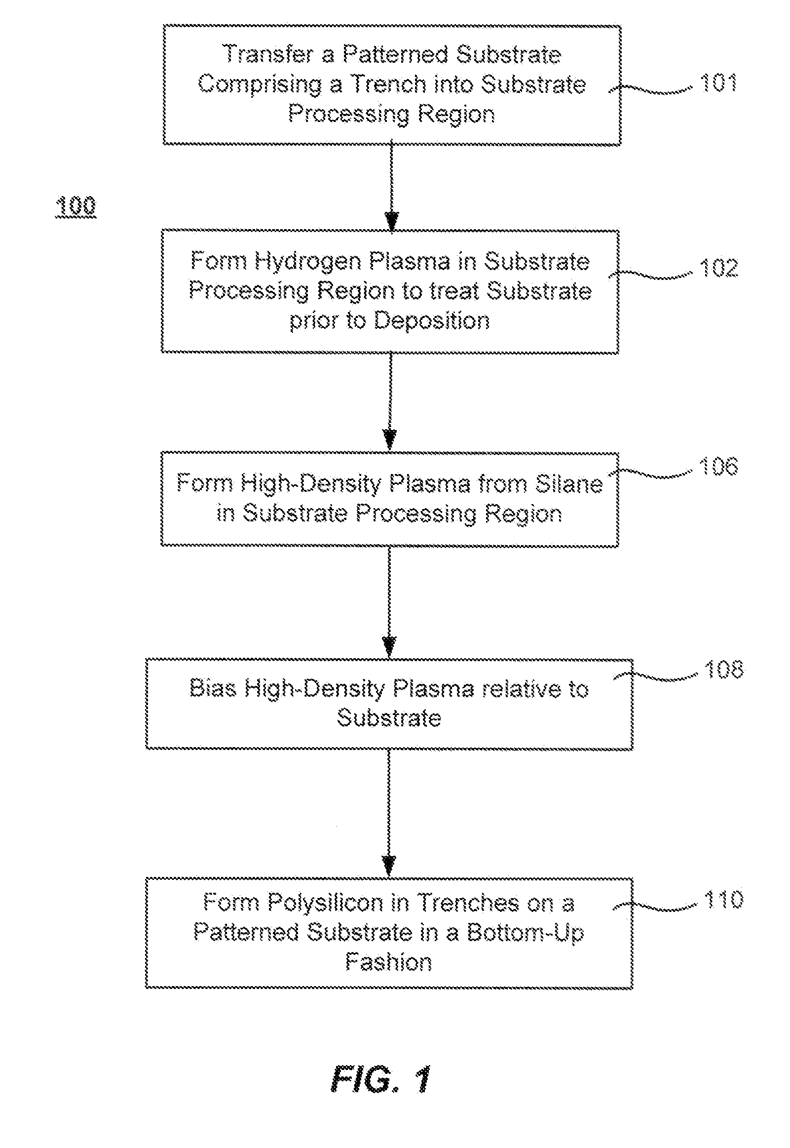
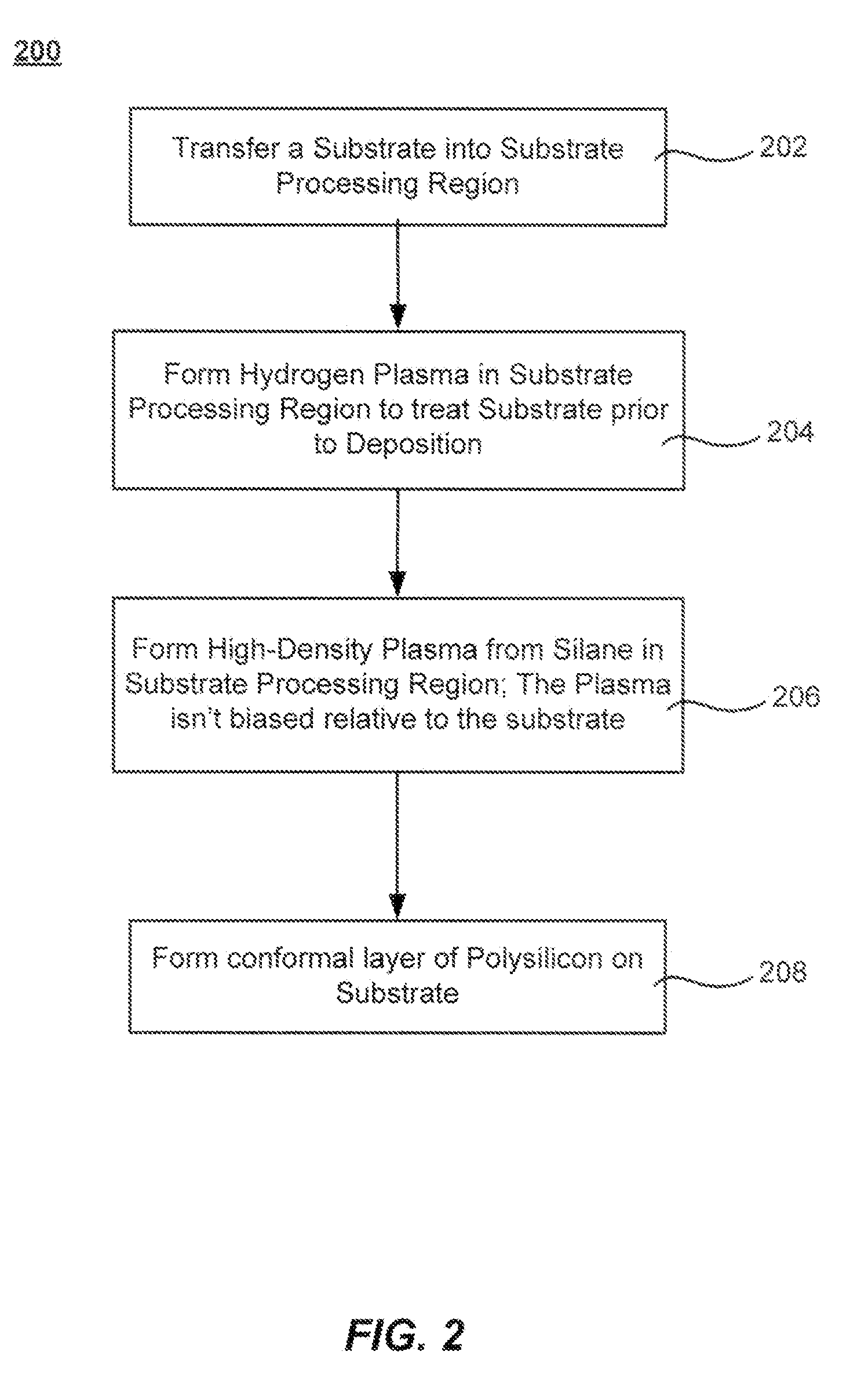
[0012]Methods of forming polysilicon layers are described. The methods include forming a high-density plasma from a silicon precursor in a substrate processing region containing the deposition substrate. The described methods produce polycrystalline films at reduced substrate temperature (e.g. <500° C.) relative to prior art techniques. The availability of a bias plasma power adjustment further enables adjustment of conformality of the formed polysilicon layer. When dopants are included in the high density plasma, they may be incorporated into the polysilicon layer in such a way that they do not require a separate activation step.

[0013]Depositing polysilicon on patterned substrate has been determined to be possible using high-density plasma techniques, with or without applied bias power. Stress typically associated with high-density plasma films has been found to be accommodated especially in systems with exposed silicon oxide on the patterned substrate. Conformal and bottom-up gapf...


PUM

PropertyMeasurementUnit
temperatureaaaaaaaaaa
feature sizesaaaaaaaaaa

Abstract

Methods of forming polysilicon layers are described. The methods include forming a high-density plasma from a silicon precursor in a substrate processing region containing the deposition substrate. The described methods produce polycrystalline films at reduced substrate temperature (e.g. <500° C.) relative to prior art techniques. The availability of a bias plasma power adjustment further enables adjustment of conformality of the formed polysilicon layer. When dopants are included in the high density plasma, they may be incorporated into the polysilicon layer in such a way that they do not require a separate activation step.

Description

CROSS-REFERENCES TO RELATED APPLICATIONS[0001]This application claims the benefit of U.S. Prov Pat. App. No. 61 / 435,487 filed Jan. 24, 2011, and titled “DEPOSITION OF POLYSILICON FILM BY HDP-CVD,” which is entirely incorporated herein by reference for all purposes.BACKGROUND OF THE INVENTION[0002]Semiconductor device geometries have dramatically decreased in size since their introduction several decades ago. Modern semiconductor fabrication equipment routinely produces devices with 45 nm, 32 nm, and 28 nm feature sizes, and new equipment is being developed and implemented to make devices with even smaller geometries. The decreasing feature sizes result in structural features on the device having decreased spatial dimensions. The widths of gaps and trenches on the device narrow to a point where the aspect ratio of gap depth to its width becomes high enough to make it challenging to fill the gap with material.[0003]Polycrystalline silicon (often shortened to polysilicon) is a material...

Claims


Application Information

Patent Timeline
Patent Type & Authority Patents(United States)
IPC IPC(8): H01L21/20H01L21/3205
CPCH01L21/02529H01L21/02532H01L21/02573H01L21/02595H01L21/0262H01L21/28556C23C16/0245C23C16/045C23C16/24
Inventor WANG, ANCHUANCHEN, XIAOLINLEE, YOUNG S.
Owner APPLIED MATERIALS INC
Why Eureka
Try Eureka