Eureka AIR delivers breakthrough ideas for toughest innovation challenges, trusted by R&D personnel around the world.

Multilayer wiring substrate

a multi-layer wiring and substrate technology, applied in the field of multi-layer wiring substrates, can solve the problems of warpage and insufficient elimination of shrinkage differences, and achieve the effects of reducing shrinkage, reducing warpage, and reducing shrinkag

Inactive Publication Date: 2013-05-28
NGK SPARK PLUG CO LTD
View PDF8 Cites 2 Cited by
  • Summary
  • Abstract
  • Description
  • Claims
  • Application Information

AI Technical Summary

Benefits of technology

[0011]The present invention has been conceived in view of the above problem, and an object of the invention is to provide a multilayer wiring substrate whose warpage is restrained through reduction of the difference in shrinkage between a main face side on which a chip component is mounted and a back face side opposite the main face side.
[0013]According to the invention described in Means 1, in a multilayer wiring substrate in which a plurality of resin insulation layers and a plurality of conductor layers are laminated, when a resin insulation layer determined to be located at the center in consideration of the number of resin insulation layers formed of the same material is considered as a center layer, the degree of fineness of wiring patterns of conductor layers increases toward the main face side to which a chip component is surface-connected, and the number of inter-wiring spaces also increases toward the main face side. Therefore, the average of area ratios of back-face-side conductor layers provided on the back face side becomes greater than the average of area ratios of main-face-side conductor layers provided on the main face side. Notably, the area ratio of a conductor layer is an area ratio (=S1 / S2) obtained by dividing a projection area S1 of the conductor layer, which is an area of the conductor layer projected in the lamination direction, by a projection area S2 of the main face (the area of the main face projected in the lamination direction). In the multilayer wiring substrate, if all the resin insulation layers are formed to have the same thickness, since the area ratios of the back-face-side conductor layers are high, the ratio of the resin insulation layers on the main face side becomes greater than that on the back face side. The resin insulation layers shrink to a greater degree as compared with the conductor layers. Therefore, if the ratio of the resin insulation layers provided on the main face side in relation to the center layer differs from the ratio of the resin insulation layers provided on the back face side in relation to the center layer, warpage occurs due to a difference in shrinkage between the two sides. In contrast, in the present invention, of the resin insulation layers made of the same material, a plurality of resin insulation layers provided on the back face side in relation to the center layer are formed such that the average of their thicknesses becomes greater than the average of thicknesses of a plurality of resin insulation layers provided on the side toward the main face in relation to the center layer. Therefore, the difference in shrinkage between the main face side and the back face side can be reduced. As a result, warpage of the multilayer wiring substrate generated due to the difference in shrinkage can be restrained.
[0015]Preferably, of the plurality of back-face-side resin insulation layers (the resin insulation layers provided on the side toward the back face), at least one resin insulation layer in contact with a conductor layer functioning as a ground layer is thicker than the front-face-side resin insulation layers (the resin insulation layer provided on the side toward the main face). On the back face side of the multilayer wiring substrate, there is formed a conductor layer having a large area ratio and functioning as a ground layer. By means of forming a resin insulation layer in contact with one side of the ground layer or resin insulation layers in contact with opposite sides of the ground layer to be thicker than the resin insulation layers on the main face side, warpage of the multilayer wiring substrate can be restrained reliably. Notably, preferably, the resin insulation layer in contact with the ground layer is formed to have a thickness which is at least 30% greater than that of the resin insulation layers on the main face side. When this configuration is employed, warpage of the multilayer wiring substrate can be restrained more reliably.
[0016]Preferably, of the back-face-side conductor layers (conductor layers provided on the side toward the back face), at least one conductor layer functioning as a ground layer is thicker than the front-face-side conductor layers (conductor layers provided on the side toward the main face). By means of forming the ground layer on the back face side to be thicker than the conductor layers on the main face side, the strength of the wiring substrate is increased, whereby warpage of the wiring substrate can be restrained. In particular, warpage of the wiring substrate can be restrained reliably by means of forming a ground layer provided at a position near the center layer to be thicker. Notably, preferably, the ground layer is formed to have a thickness which is at least 30% greater than that of the conductor layers on the main face side. When this configuration is employed, warpage of the multilayer wiring substrate can be restrained more reliably. Preferably, the ground layer has an area ratio of 80% or higher. When this configuration is employed, a multilayer wiring substrate having an excellent electrical characteristic can be realized.

Problems solved by technology

Since the resin insulation layers and the conductor layers differ in coefficient of thermal expansion, during manufacture of the multilayer wiring substrate, a difference in shrinkage arises between the side on which an IC chip is mounted and the side to which a motherboard is connected, with resultant generation of warpage.
However, this configuration cannot sufficiently eliminate the difference in shrinkage which changes in accordance with the area ratios of the conductor layers.
Therefore, if the ratio of the resin insulation layers provided on the main face side in relation to the center layer differs from the ratio of the resin insulation layers provided on the back face side in relation to the center layer, warpage occurs due to a difference in shrinkage between the two sides.

Method used


Image

  • Multilayer wiring substrate
  • Multilayer wiring substrate
  • Multilayer wiring substrate

Examples


Embodiment Construction

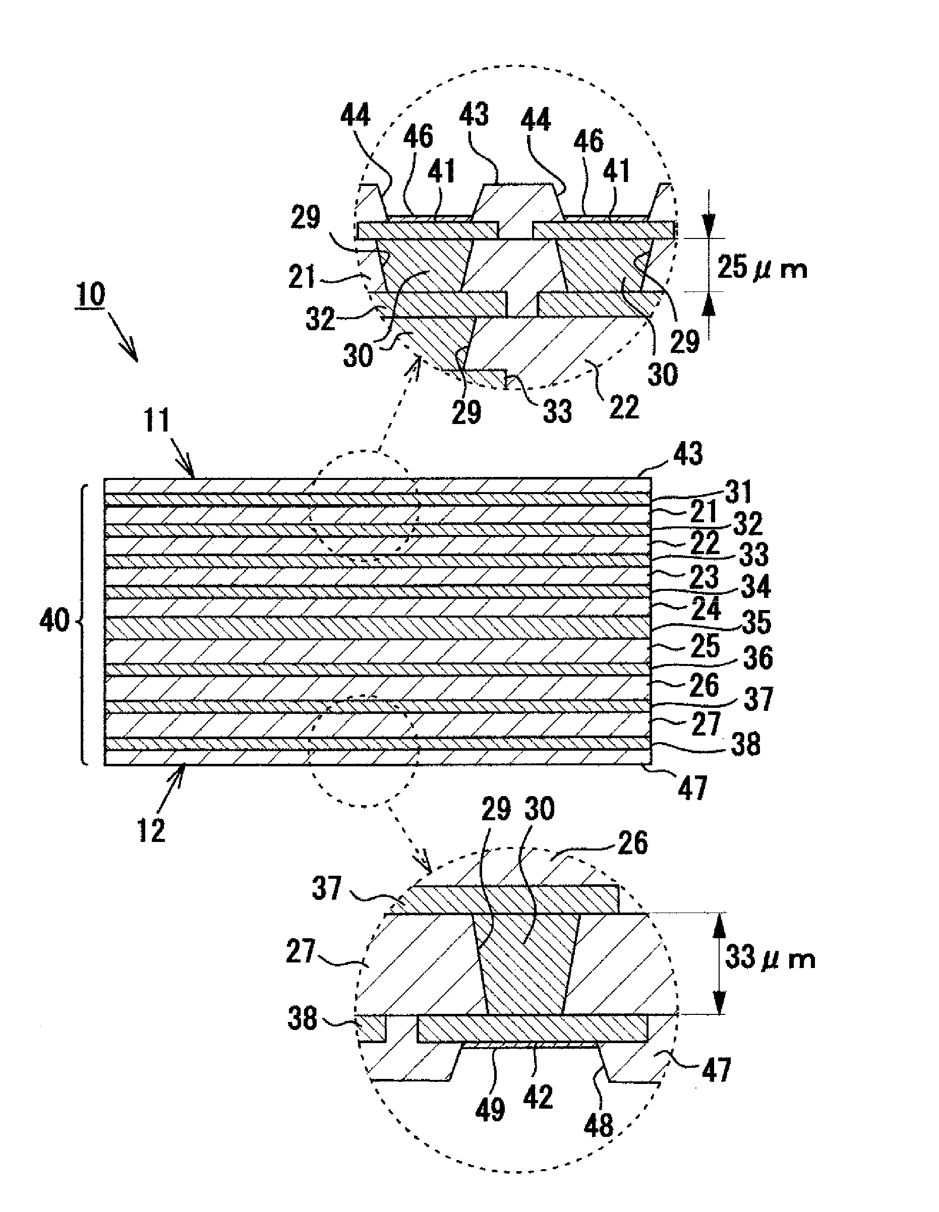
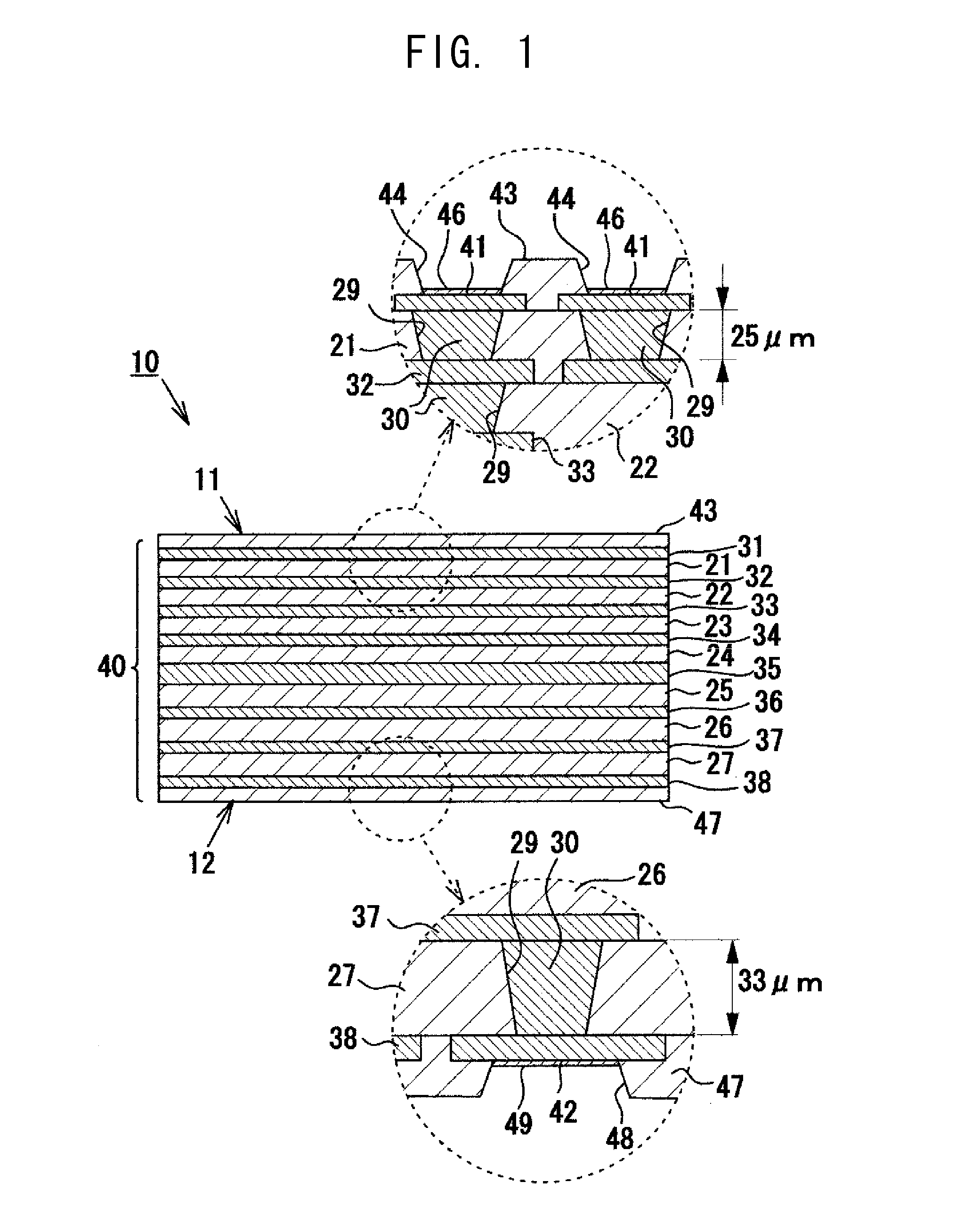
[0025]An embodiment in which the multilayer wiring substrate of the present invention is embodied will next be described in detail with reference to the drawings. FIG. 1 is a sectional view schematically showing the structure of a multilayer wiring substrate 10 according to the present embodiment.

[0026]As shown in FIG. 1, the multilayer wiring substrate 10 according to the present embodiment is a wiring substrate for mounting an IC chip. The multilayer wiring substrate 10 has a main face 11 (upper surface in FIG. 1), which serves as an IC-chip mounting face, and a back face 12 (lower surface in FIG. 1) opposite the main face 11. Specifically, the multilayer wiring substrate 10 is a coreless wiring substrate having no substrate core and has a multilayer wiring laminate portion 40 in which resin insulation layers 21, 22, 23, 24, 25, 26, and 27 made primarily of the same resin insulation material, and conductor layers 31, 32, 33, 34, 35, 36, 37, and 38 made of copper are laminated alte...


PUM


Abstract

A multilayer wiring substrate has a main face and a back face, and a configuration in which a plurality of resin insulation layers and a plurality of conductor layers are laminated. A plurality of conductor layers provided on the side toward the back face in relation to a resin insulation layer serving as a center layer are formed such that the average of their area ratios becomes greater than the average of area ratios of a plurality of conductor layers provided on the side toward the main face in relation to the center layer. A plurality of resin insulation layers provided on the side toward the back face are formed such that the average of their thicknesses becomes greater than the average of thicknesses of a plurality of resin insulation layers provided on the side toward the main face.

Description

CROSS REFERENCE TO RELATED APPLICATIONS[0001]The present application claims priority from Japanese Patent Application No. 2010-247114, which was filed on Nov. 4, 2010, the disclosure of which is herein incorporated by reference in its entirety.BACKGROUND OF THE INVENTION[0002]1. Field of the Invention[0003]The present invention relates to a multilayer wiring substrate having a multilayer structure in which a plurality of resin insulation layers and a plurality of conductor layers are laminated alternately.[0004]2. Description of Related Art[0005]In association with recent increasing tendency toward higher operation speed and higher functionality of semiconductor integrated circuit devices (IC chips) used as, for example, microprocessors of computers, the number of terminals increases, and the pitch between the terminals tends to become narrower. Generally, a large number of terminals are densely arrayed on the bottom surface of an IC chip and flip-chip-bonded to terminals provided o...

Claims


Application Information

Patent Timeline
Patent Type & Authority Patents(United States)
IPC IPC(8): H05K1/03
CPCH01L23/49822H05K3/4682H05K2201/0191H05K2201/09136H05K2201/0352H01L2924/0002H01L2924/00H05K3/46
Inventor MAEDA, SHINNOSUKE
Owner NGK SPARK PLUG CO LTD
Why Eureka
Eureka Blog
Learn More