3-level pulse width modulation inverter with snubber circuit

a pulse width modulation and inverter technology, applied in the direction of power electronics conversion, climate sustainability, power conversion systems, etc., can solve the problems of snubber circuit, loss of parts, etc., and achieve the effect of favorable pulse control methods, small and lightweight, and simple design

Inactive Publication Date: 2013-06-11
HOCHSCHULE KONSTANZ
View PDF14 Cites 7 Cited by
  • Summary
  • Abstract
  • Description
  • Claims
  • Application Information

AI Technical Summary

Benefits of technology

[0019]In the proposed circuit arrangement, all the switching losses are completely avoided as a matter of principle. Through the simple design of the snubber circuit, which in a preferred embodiment comprises a coil, two capacitors and four diodes, the circuit arrangement can be produced very cost-effectively, small and lightweight. No additional expensive power semiconductors able to be switched on and off and therefore also no expensive control circuits are required. The duration of the discharge function of the proposed snubber circuit is dependent only to a small extent on the load current and is therefore favorable for pulse control methods. The circuit arrangement has the further advantage of a robust and error-tolerant control without the risk of malfunctions. In an additional expansion phase, wherein the outer switching elements in particular are suitably triggered, the circuit arrangement is also very EMC-friendly (EMC: electromagnetic compatibility), since the gradient du / dt of the generated voltage pulses can easily be limited to non-critical values of du / dt<1 kV / μs.

Problems solved by technology

The snubber circuit, however, operates in a manner involving a loss, i.e. it produces for its part losses which as a rule are greater than the saved switching losses.
An improvement in the efficiency is not therefore possible.
This makes the pulse control process difficult.
They are however very complex and expensive.
Moreover, the control of the power semiconductors, now totaling eight, is very complicated.
Components can be destroyed even in the case of only a slight faulty control.
The circuit arrangement, however, has a poor overall efficiency and displays huge limitations in controllability.

Method used


Image

  • 3-level pulse width modulation inverter with snubber circuit
  • 3-level pulse width modulation inverter with snubber circuit
  • 3-level pulse width modulation inverter with snubber circuit

Examples


Embodiment Construction

[0014]The object is achieved with the circuit arrangement according to claim 1. Advantageous embodiments of the circuit arrangement are subject-matter of the dependent claims or can be derived from the following description and the examples of embodiment.

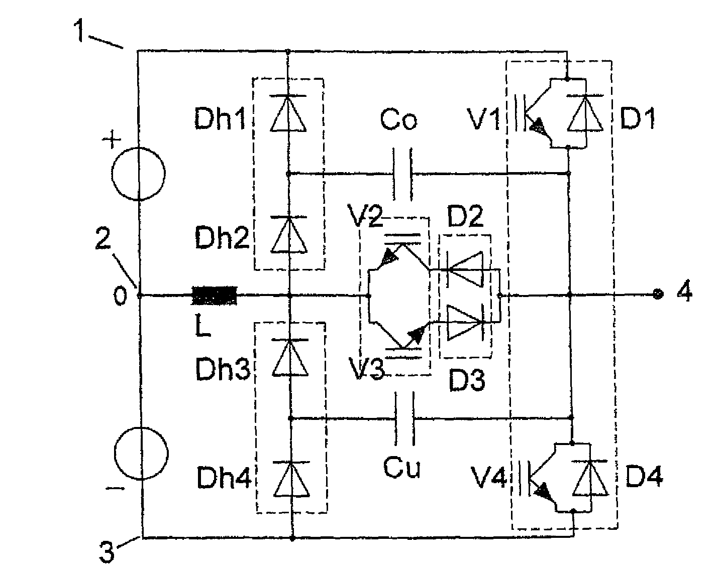
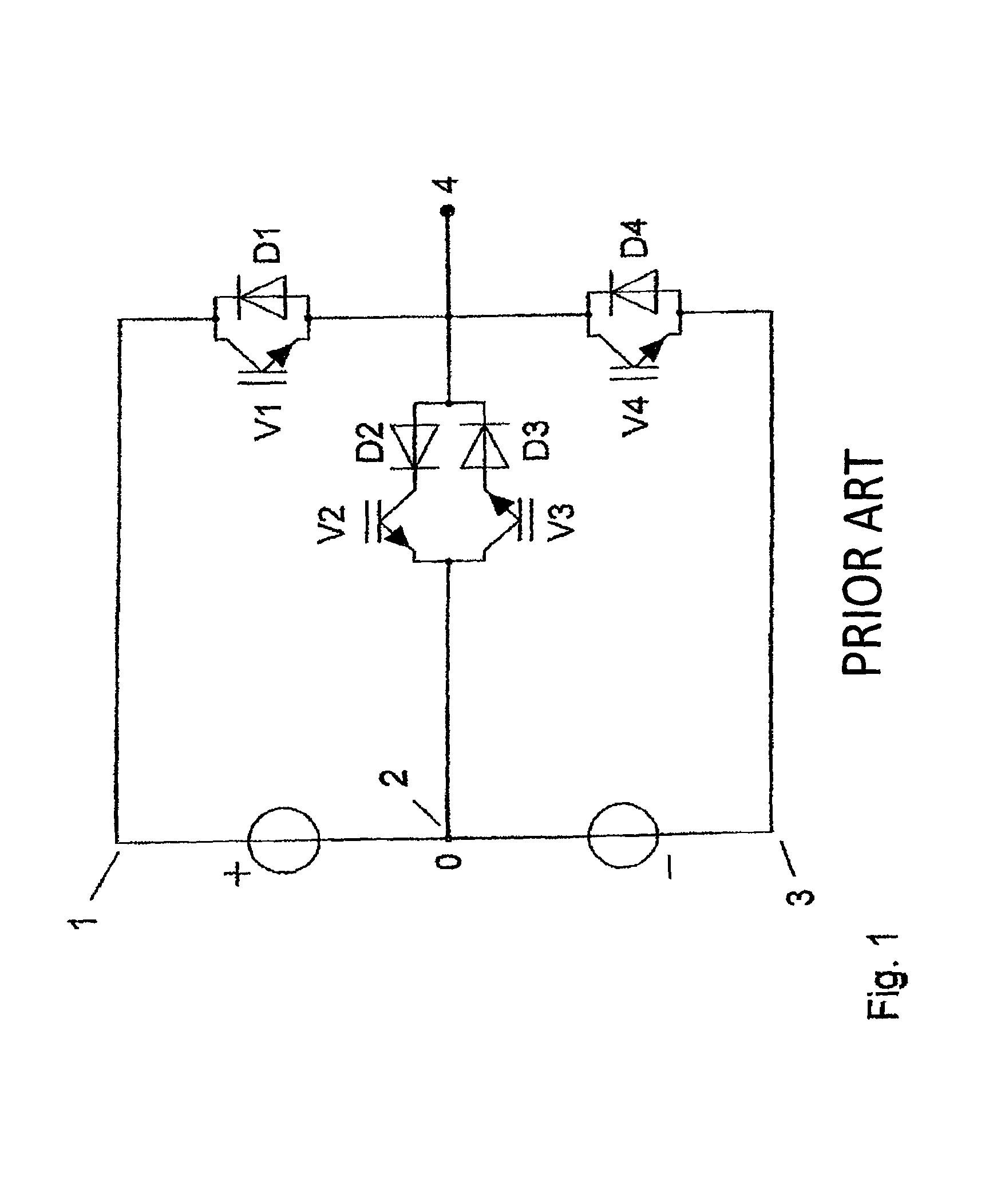
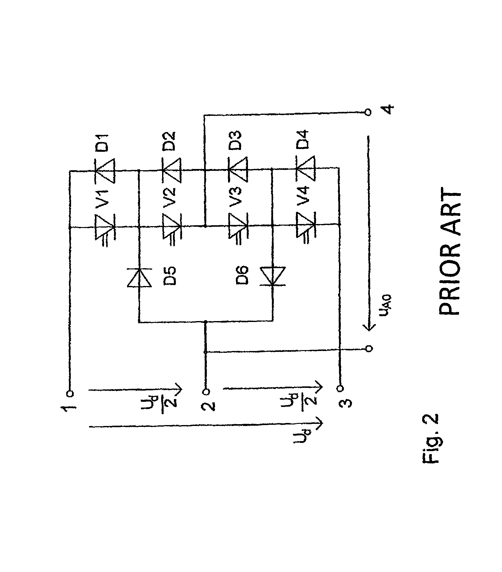
[0015]The proposed circuit arrangement comprises at least one 3-level pulse width modulation inverter with a snubber circuit and input terminals for a positive pole, a negative pole and a centre tap of an input voltage as well as an output terminal, at which the pulsed output voltage of the pulse width modulation inverter can be tapped. The 3-level pulse width modulation inverter is designed in a known manner, i.e. it comprises at least two outer switching elements, which are connected to the input terminals for the positive and the negative pole of the input voltage, and two inner switching elements, which are connected to the output terminal. Known switching topologies of 3-level pulse width modulation inverters can be implemented...


PUM


Abstract

The present invention relates to a circuit arrangement which comprises at least one 3-level pulse width modulation inverter with a snubber circuit. The snubber circuit is formed by at least one coil (L), two capacitors (Cu, Co) and a series connection comprising four diodes (Dh1-Dh4) poled in the same direction, whereof the two outer diodes (Dh1, Dh4) are in each case directly connected to the input terminals (1, 3) for the positive and the negative pole of the input voltage. The electrical connection between the two inner diodes (Dh2, Dh3) is connected on the one hand via the coil (L) to the input terminal (2) for the center tap of the input voltage and on the other hand to the middle bridge branch of the pulse width modulation inverter. In one embodiment, the two capacitors (Cu, Co) are in each case connected with one terminal to the electrical connection between one of the inner diodes (Dh2, Dh3) and one of the outer diodes (Dh1, Dh4) and with the other terminal directly to the output terminal (4).With the proposed circuit, switching losses are completely avoided as a matter of principle with a simple and low-cost design.

Description

TECHNICAL FIELD OF APPLICATION[0001]The present invention relates to a circuit arrangement which comprises at least one 3-level pulse width modulation inverter with a snubber circuit and comprises input terminals for a positive pole, a negative pole and a centre tap of an input voltage as well as an output terminal, wherein the pulse width modulation inverter comprises at least two outer switching elements, which are connected to the input terminals for the positive and the negative pole of the input voltage, and two inner switching elements, which are connected to the output terminal. In such a circuit arrangement, the snubber circuit serves to reduce the switching losses of the pulse width modulation inverter.[0002]Pulse width modulation inverters generate from a direct voltage source one or more pulsed voltages, which apart from the pulse frequency (several kHz up to over 20 kHz) have a fundamental oscillation with an adjustable frequency (0 to approx. 500 Hz) and an adjustable e...

Claims


Application Information

Patent Timeline
Patent Type & Authority Patents(United States)
IPC IPC(8): H02H7/122H02M1/06H02M7/515H02M7/521
CPCH02M7/487H02M1/34Y02B70/1491H02M2001/342H02M1/342H02M7/483H02M1/32H02M1/0048Y02B70/10
Inventor GEKELER, MANFRED W.
Owner HOCHSCHULE KONSTANZ
Why Eureka
Try Eureka