Electrophotographic photosensitive member and electrophotographic apparatus

a photosensitive member and electrophotography technology, applied in the direction of electrographic process apparatus, instruments, corona discharge, etc., can solve the problems of image failure, letter blurred or white patches without being printed, occasionally caused image deletion, etc., to achieve superior resistance to high-humidity deletion, abrasion resistance and layer exfoliation resistance

Inactive Publication Date: 2013-06-18
CANON KK
View PDF47 Cites 3 Cited by
  • Summary
  • Abstract
  • Description
  • Claims
  • Application Information

AI Technical Summary

Benefits of technology

[0014]An object of the present invention is to provide an electrophotographic photosensitive member having superior resistance to high-humidity deletion, abrasion resistance and resistance to layer exfoliation, and an electrophotographic apparatus having the electrophotographic photosensitive member.
[0016]The present invention can provide an electrophotographic photosensitive member having superior resistance to high-humidity deletion, abrasion resistance and resistance to layer exfoliation, and an electrophotographic apparatus having the electrophotographic photosensitive member.

Problems solved by technology

However, a conventional a-SiC surface layer has occasionally caused an image deletion (hereinafter referred to as “high-humidity deletion” as well) when having been used in a high-humidity environment.
The high-humidity deletion means such an image failure that letters are blurred or form a white patch without being printed, occurring when an image has been repeatedly formed in the high-humidity environment according to an electrophotographic process and an image is output again after a while.
One cause of this phenomenon is moisture which has adsorbed onto the surface of the electrophotographic photosensitive member.
Here, when the above described heater for the photosensitive member is installed so as to keep the high image quality in the high-humidity environment, an electric power corresponding to a standby power is needed even when the electrophotographic apparatus is not operated, which makes it difficult to improve the power-saving properties.
In addition, even when the technology disclosed in Japanese Patent No. 3124841 is employed, the surface of the electrophotographic photosensitive member needs to be scraped off at some abrasion rate, and accordingly, an electrophotographic apparatus having a quick process speed, in particular, does not sufficiently secure the durability of the electrophotographic photosensitive member, occasionally.
However, when the surface layer having a large internal stress has been used, even though the above described intermediate layer was provided, there has been the case in which the interface between the photoconductive layer and the intermediate layer cannot withstand the high stress received from the surface layer, and the layer exfoliation occurs in the vicinity of the interface.
In addition even if the layer exfoliation in the vicinity of the interface between the photoconductive layer and the a-SiC surface layer is reduced by providing the intermediate layer, there has been the case of causing the layer exfoliation due to the fracture of the photoconductive layer when a sudden environmental change has occurred.

Method used


Image

  • Electrophotographic photosensitive member and electrophotographic apparatus
  • Electrophotographic photosensitive member and electrophotographic apparatus
  • Electrophotographic photosensitive member and electrophotographic apparatus

Examples


experimental example 1

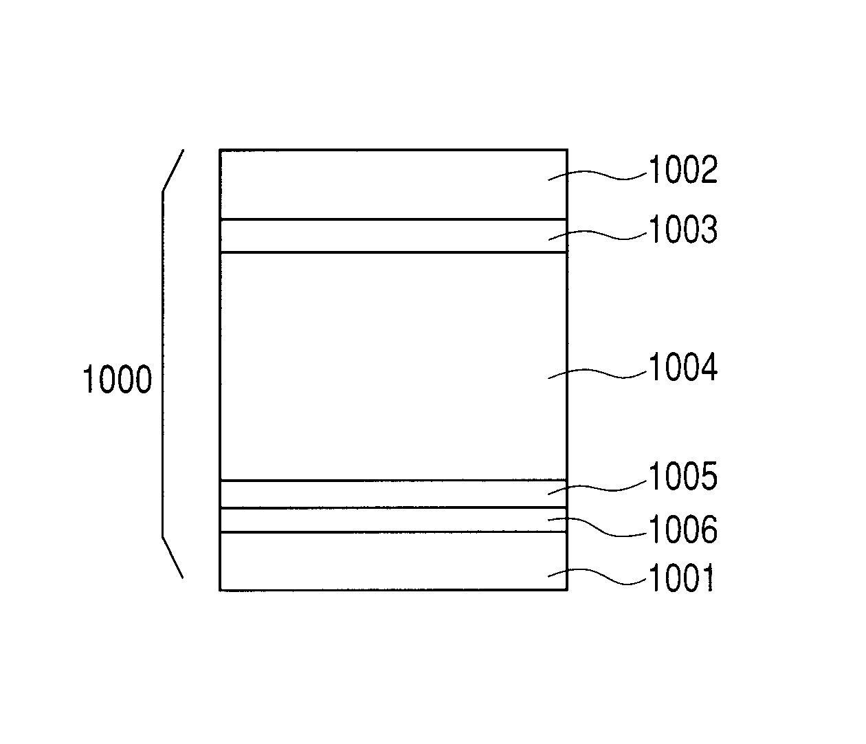
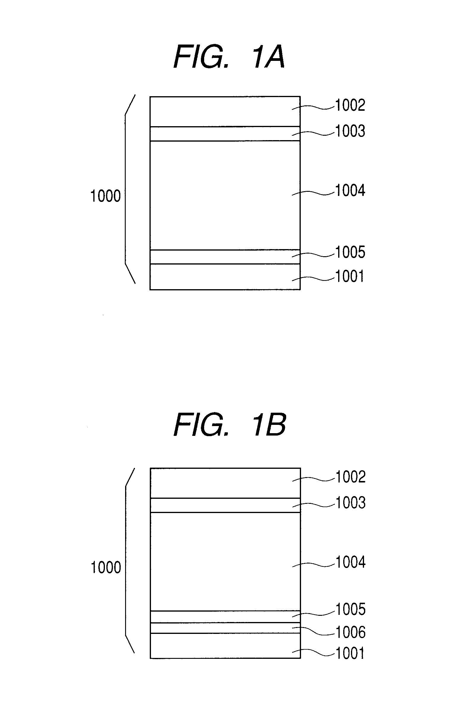
[0084]A sample of the electrophotographic photosensitive member was produced by forming each layer on a cylindrical substrate (cylindrical substrate made from aluminum, which had a diameter of 80 mm, a length of 358 mm and a thickness of 3 mm, and was mirror-finished) by using a plasma treatment apparatus with the use of a high-frequency power source illustrated in FIG. 3, which uses an RF band. The forming conditions of a charge injection inhibition layer at this time are shown in the following Table 1, the forming conditions of a photoconductive layer are shown in the following Table 2, the forming conditions of an intermediate layer are shown in the following Table 3, the forming conditions of a surface layer are shown in the following Table 4, and the stacking conditions in the samples of the produced electrophotographic photosensitive member are shown in the following Table 5. As for the layer structures of the electrophotographic photosensitive members shown in the following t...

examples 8 to 12

[0152]Positively chargeable a-Si photosensitive members were produced on a cylindrical substrate, on conditions of the following Tables 28 to 33, in a similar way to those in Experimental Example 1. At this time, the adhesive layer and the charge injection inhibition layer were formed on conditions shown in the following Table 27. In addition, the produced number of electrophotographic photosensitive members was two cylinders for each layer-forming condition (film-forming condition).

[0153]

TABLE 27Layer-formingLayer-formingconditioncondition No. ofNo. of adhesivecharge injectionlayerinhibition layerN1U1U2U3SiH4 [mL / min (normal)]350350350350H2 [mL / min (normal)]750750750750B [ppm] (with respect to Si)1500150015001500NO [mL / min (normal)]——10—CH4 [mL / min (normal)]———500N2 [mL / min (normal)]750———High-frequency electric power (W)400400400400Internal pressure (Pa)40404040Substrate temperature (° C.)260260260260

[0154]

TABLE 28Example 8Layer-ChargePhotoconductive layerIntermediate layerSurface...


PUM


Abstract

An electrophotographic photosensitive member includes a photoconductive layer, an intermediate layer, and a surface layer. When Si+C atom density in the surface layer is represented by DS×1022 atoms / cm3, the DS is 6.60 or more, and when the maximal value of H / (Si+H) in a distribution of hydrogen quantity in the photoconductive layer in a layer thickness direction is represented by HPmax, the average value of the H / (Si+H) in the second photoconductive region is represented by HP2, the DS and the HP2 satisfy the following expression (1) and the DS and the HPmax satisfy the following expression (2).HP2≧0.07×DS−0.38  Expression (1)HPmax≦0.04×DS+0.60  Expression (2)

Description

BACKGROUND OF THE INVENTION[0001]1. Field of the Invention[0002]The present invention relates to an electrophotographic photosensitive member and an electrophotographic apparatus. The present invention specifically relates to an electrophotographic photosensitive member which has a photoconductive layer formed from hydrogenated amorphous silicon, and has an intermediate layer and a surface layer both of which are formed from hydrogenated amorphous silicon carbide, on the photoconductive layer. Hereinafter, the hydrogenated amorphous silicon is referred to as “a-Si” as well, and the hydrogenated amorphous silicon carbide is referred to as “a-SiC” as well. In addition, the surface layer formed from “a-SiC” is referred to as “an a-SiC surface layer” as well.[0003]2. Description of the Related Art[0004]An electrophotographic photosensitive member is known, which has a photoconductive layer (photosensitive layer) formed from an amorphous material on a substrate. An amorphous-silicon elec...

Claims


Application Information

Patent Timeline
Patent Type & Authority Patents(United States)
IPC IPC(8): G03G5/00
CPCG03G5/0433G03G5/14704G03G5/144G03G5/08235
Inventor OZAWA, TOMOHITOAKIYAMA, KAZUYOSHINISHIMURA, YUUTAZAWA, DAISUKE
Owner CANON KK
Why Eureka
Try Eureka