Display device, control device of display device, driving method of display device, liquid crystal display device, and television receiver

a display device and control device technology, applied in the direction of static indicating devices, instruments, television systems, etc., can solve the problem of difficult recognition of the border between the respective regions, and achieve the effect of reducing the difference in luminan

Inactive Publication Date: 2013-07-16
SHARP KK
View PDF20 Cites 9 Cited by
  • Summary
  • Abstract
  • Description
  • Claims
  • Application Information

AI Technical Summary

Benefits of technology

[0005]The present invention is accomplished in view of the problem, and its object is to provide a configuration which can prevent a difference in luminance between respective regions in a display device in which a display section is divided into a plurality of regions and the respective plurality of regions are separately driven.
[0007]According to the configuration, in a case where the first region has luminance different from that of the second region even when the regions are displayed in an identical tone, the difference in luminance can be reduced, with the use of the waveform adjusting section, by causing the first scan signal to have a waveform, during an active period, which is different from a waveform which the second scan signal has during an active period. This makes it difficult for a border between the respective regions to be recognized.
[0011]The display device may include a memory which stores the adjusting data. With the configuration, the adjustment data can be conveniently set up by writing the data into the memory.
[0012]According to the display device, the waveform adjusting section may cause the first scan signal to have a width of an active period which is different from that of the second scan signal.
[0014]According to the display device, the waveform adjusting section may cause the first scan signal to have a start timing of the falling edge which start timing is different from a start timing of the falling edge of the second scan signal.
[0038]As described above, according to the display device, in a case where the first and second regions have different luminance even when the regions are displayed in an identical tone, the waveform adjusting section causes the first scan signal to have a waveform, during an active period, which is different from a waveform which the second scan signal has during an active period. This makes it possible to reduce the difference in luminance.

Problems solved by technology

This makes it difficult for a border between the respective regions to be recognized.

Method used


Image

  • Display device, control device of display device, driving method of display device, liquid crystal display device, and television receiver
  • Display device, control device of display device, driving method of display device, liquid crystal display device, and television receiver
  • Display device, control device of display device, driving method of display device, liquid crystal display device, and television receiver

Examples


embodiment 1

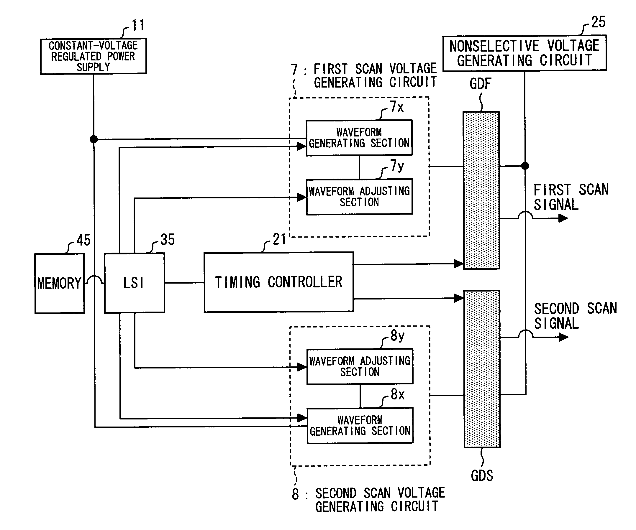
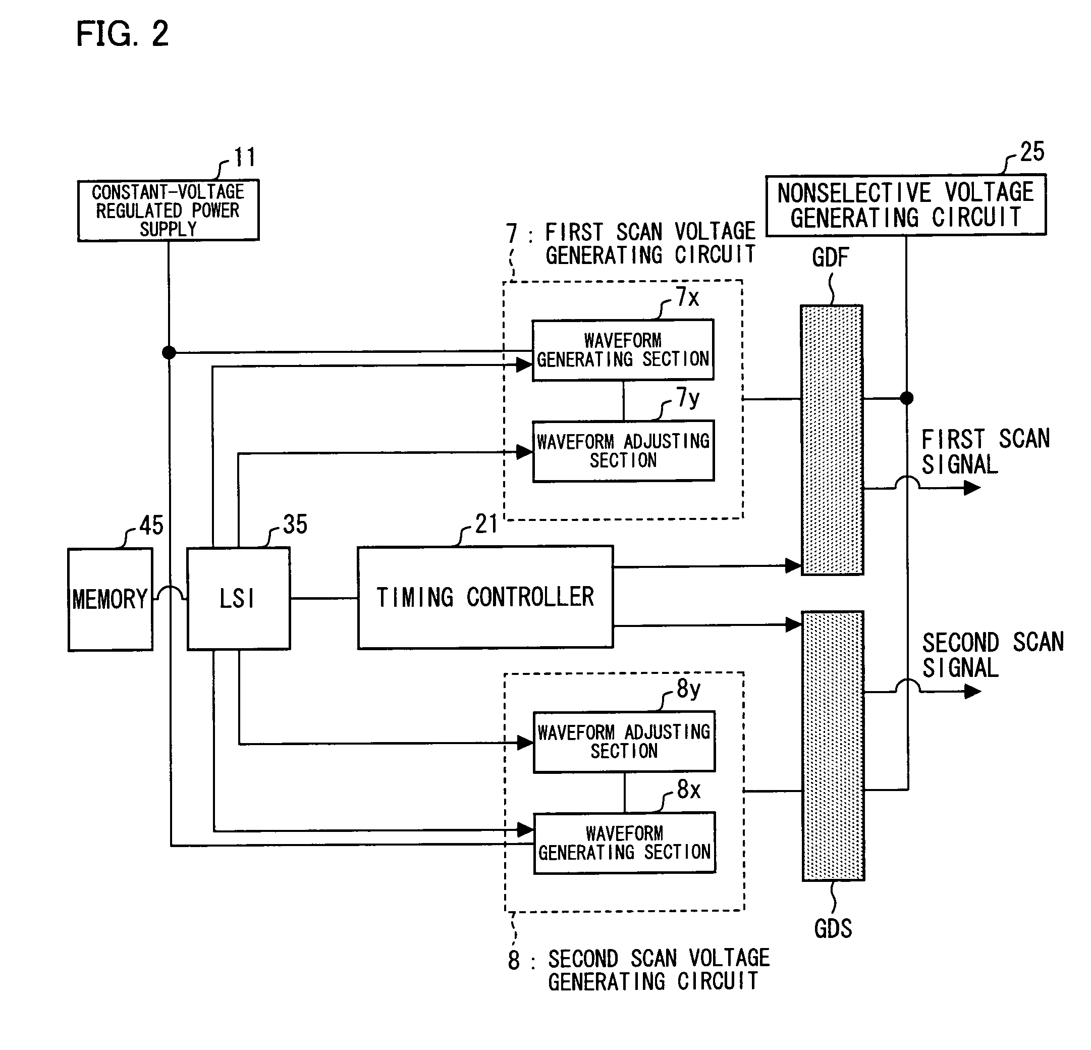
[0093]FIG. 2 is a block diagram illustrating a part of the driver control circuit 3 shown in FIG. 1 and the first and second gate drivers GDF and GDS. As shown in FIG. 2, the driver control circuit 3 includes: a constant-voltage regulated power supply 11; a nonselective voltage generating circuit 25; a memory 45; an LSI 35 (a waveform adjusting section controlling circuit); a timing controller 21; a first scan voltage generating circuit 7; and a second scan voltage generating circuit 8. Note that the first scan voltage generating circuit 7 includes a waveform generating section 7x and a waveform adjusting section 7y, and the second scan voltage generating circuit 8 includes a waveform generating section 8x and a waveform adjusting section 8y.

[0094]The first scan voltage generating circuit 7 converts a constant voltage supplied from the constant-voltage regulated power supply 11 so that the converted voltage corresponds to the first region FA, and outputs to the first gate driver GD...

embodiment 2

[0108]FIG. 9 is a block diagram illustrating a part of the driver control circuit 3 and first and second gate drivers GDF and GDS shown in FIG. 1. As shown in FIG. 9, the driver control circuit 3 includes: a constant-voltage regulated power supply 11; a nonselective voltage generating circuit 25; a memory 45; an LSI 35; a timing controller 21; a first scan voltage generating circuit 7; and a second scan voltage generating circuit 8. Note that the first scan voltage generating circuit 7 includes a waveform generating section 7x and a waveform adjusting section 7y, and the second scan voltage generating circuit 8 includes a waveform generating section 8x and a waveform adjusting section 8y.

[0109]The first scan voltage generating circuit 7 converts a constant voltage supplied from the constant-voltage regulated power supply 11 so that the converted voltage corresponds to the first region FA, and outputs to the first gate driver GDF, as a first scan voltage, the converted voltage. More...

embodiment 3

[0124]In the present embodiment, as shown in FIG. 17, (i) a subsequent stage circuit 10 shown in FIG. 10 is provided so as to follow the waveform generating section 7x shown in FIG. 11 and a subsequent stage circuit 10 shown in FIG. 10 is provided so as to follow the waveform generating section 8x shown in FIG. 11. That is, the subsequent stage circuit 10 is provided between the first gate driver GDF and an emitter terminal of the transistor Tr3, and the another subsequent stage circuit 10 is provided between the second gate driver GDS and an emitter terminal of the transistor Tr3. Note that each of the subsequent stage circuits 10 includes: a transistor Tr11 which is an NPN bipolar transistor; resistors R11 and R12; a diode d; and a transistor Tr12 which is an N-channel FET. The transistor Tr12 has a source terminal which is grounded. The resistor R11 is provided between a collector terminal of the transistor Tr11 and a base terminal of the transistor Tr11. The diode d has (i) an a...


PUM


Abstract

In one embodiment of the present invention, a display device includes: a display section in which a plurality of data signal lines and a plurality of scan signal lines are provided, the display section including (i) a first region including some of the plurality of scan signal lines to which a first scan signal is sequentially supplied and (ii) a second region including the others of the plurality of scan signal lines to which a second scan signal is sequentially supplied; and waveform adjusting sections for causing the first scan signal to have a waveform, during an active period, which is different from a waveform which the second scan signal has during an active period. This allows a display device, which drives a display section divided into a plurality of regions, to reduce a difference in luminance between the regions.

Description

TECHNICAL FIELD[0001]The present invention relates to a scan signal (gate on pulse) supplied to a scan signal line of a display device.BACKGROUND ART[0002]In order to deal with (i) shortening of writing time to each pixel due to a high definition of a display device such as a liquid crystal display device and (ii) a blunt signal waveform caused by large scale of the display device, a configuration has been proposed in which a display section of the display device is divided into a plurality of regions and the regions are separately driven. For example, Patent Literature 1 discloses a display device in which a display section is divided into a first region and a second region (see FIG. 30). In the first region, a plurality of source lines (HS1 through HSm) and a plurality of gate lines (G1 through G(n / 2)) are provided. In the second region, a plurality of source lines (HS1′ through HSm′) and a plurality of gate lines (G(n / 2+1) through Gn) are provided. According to the display device...

Claims


Application Information

Patent Timeline
Patent Type & Authority Patents(United States)
IPC IPC(8): G09G3/36
CPCG09G3/3677G09G2310/0208G09G2310/021G09G2310/04G09G2320/0233G09G2320/0693
Inventor ITOH, MOTOMITSU
Owner SHARP KK
Why Eureka
Try Eureka