System and method for aligning surface mount devices on a substrate

Active Publication Date: 2013-07-23
MACOM CONNECTIVITY SOLUTIONS LLC
View PDF20 Cites 13 Cited by
  • Summary
  • Abstract
  • Description
  • Claims
  • Application Information

AI Technical Summary

Benefits of technology

[0013]The placement of optical components, such as laser diodes (e.g., vertical-cavity surface-emitting laser (VCSELs)) and photodiodes, is critical for optimal optical performance. Conventional techniques include high-accuracy low throughput pick-a

Problems solved by technology

Highly accurate pick-and-place equipment can provide tolerances down to 0.001 mm, but the equipment purchase price, maintenance requirements, and low throughput make their use prohibitively expensive for most commercial applications.
Unfortunately, high throughput pick-and-place machines do not currently have the placement accuracy to locate parts that must be stacked on top of each other with tight tolerances, such as optical system components.
The placement challenges increase with the number of components on the substrate due to systemic offsets or overall statistical variability resulting in lower product manufact

Method used


Image

  • System and method for aligning surface mount devices on a substrate
  • System and method for aligning surface mount devices on a substrate
  • System and method for aligning surface mount devices on a substrate

Examples


Example

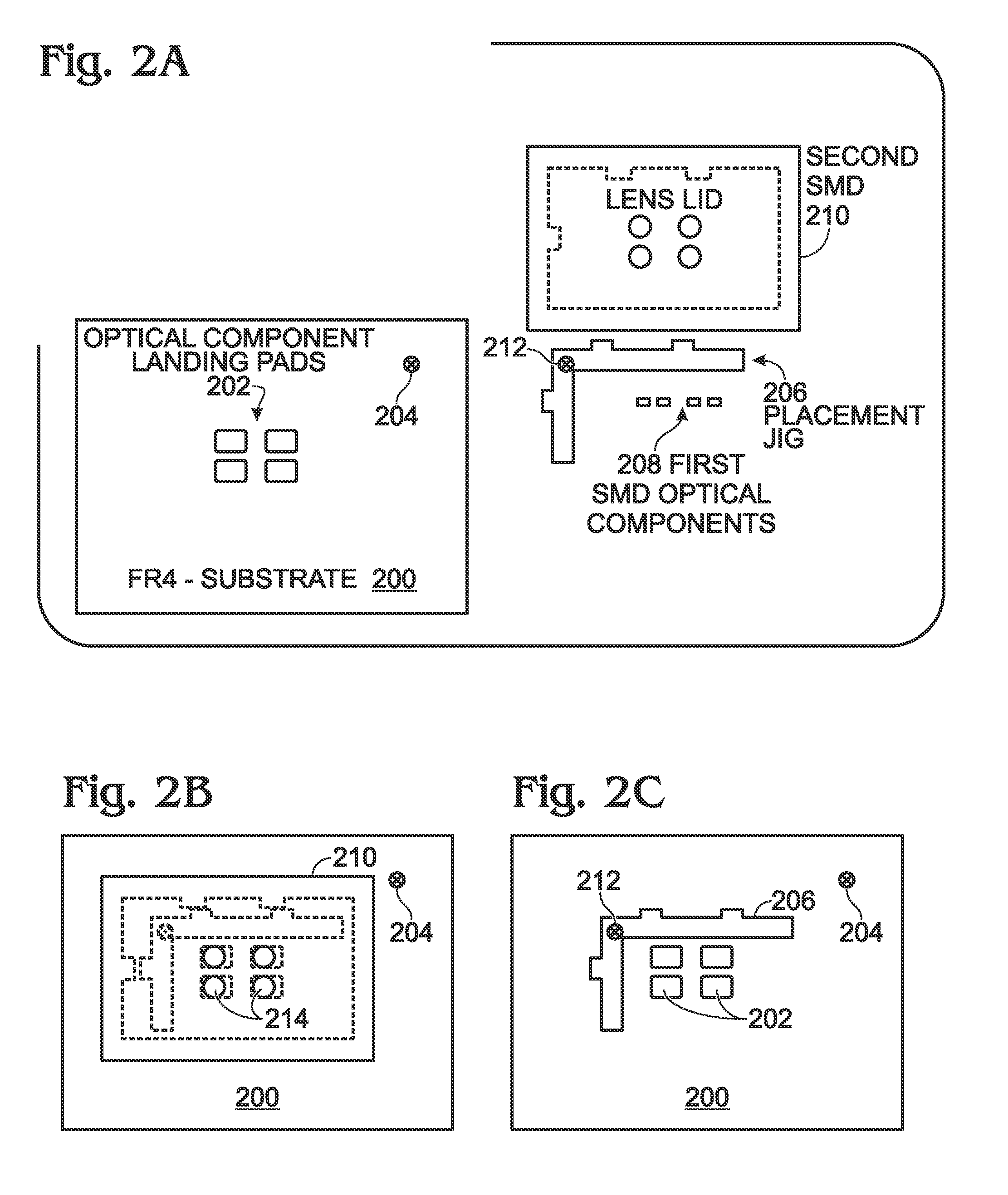
[0025]FIGS. 2A through 2H depict steps in an exemplary fabrication process using the method described in FIG. 1. FIG. 2A is a plan view depicting a substrate 200, for example a FR4 material, with 4 landing pads 202. The first reference feature 204 is a fiducial. To aid in placement, the component landing pads 202 may be substantially fiat, with no traces running underneath the landing pads. The figure also shows the components to be placed: an alignment or placement jig 206, first SMD components 208 enabled as optical components, and a second SMD 210 enabled as a lens lid. To aid in placement, the alignment jig may be built using materials that can guarantee a tighter dimensional tolerance than the placement tolerance of the placement machine. Injection molded plastics, and stamped / formed metals are examples of materials that can be used in one aspect, the first reference feature (fiducial) 204 is used for coarse alignment of the jig 206 to the substrate 200, e.g., + / −1 mil (25 micr...


PUM


Abstract

A method is provided for assembling a stack of surface-mount devices (SMDs) on a substrate. The method provides a substrate, die, or printed circuit board (PCB) with a top surface having a landing pad and a first reference feature. An alignment jig is placed overlying the substrate top surface. The alignment jig second reference feature is aligned with respect to the substrate first reference feature. A first SMD is placed overlying the substrate landing pad. The first SMD third reference feature is aligned with respect to the alignment jig second reference feature. A second SMD is placed overlying the substrate top surface. Then, the alignment jig first boundary feature is mated with the second SMD second boundary feature. In response to the mating, the second SMD first interface is aligned over an underlying SMD active element.

Description

BACKGROUND OF THE INVENTION[0001]1. Field of the Invention[0002]This invention generally relates to integrated circuit packaging and, more particularly, to a system and method for precisely aligning a stack of tightly tolerance surface mount devices such as optical components.[0003]2. Description of the Related Art[0004]As noted in Wikipedia, common commercial circuit packaging includes the dual in-line package (DIP), pin, grid array (PGA), ball grid array (BGA), leadless chip carrier (LCC) packages, and surface mount package with leads formed as either a gull-wing or J-lead. A surface mount package typically occupies an area about 30-50% less than an equivalent DIP, with a typical thickness that is 70% less. This package has “gull wing” leads protruding from the two long sides and a lead spacing of 0.050 inches. In a Flip-chip Ball Grid Array (FCBGA) package the die is mounted upside-down (flipped) and connects to the package balls via a package substrate that is similar to a print...

Claims


Application Information

Patent Timeline
IPC IPC(8): G01R31/26
CPCG01R31/2635
Inventor FANFELLE, ROBERT JAMES
Owner MACOM CONNECTIVITY SOLUTIONS LLC
Why Eureka
Try Eureka