Method of manufacturing thin-film light-absorbing layer, and method of manufacturing thin-film solar cell using the same

a technology of solar cells and light-absorbing layers, which is applied in the field of manufacturing a thin-film light-absorbing layer and a manufacturing method of a thin-film solar cell using the same, can solve the problems of large-area solar cell production, difficult to make one with a large area, and expensive equipment, and achieves the effect of simple and inexpensive manufacturing

Inactive Publication Date: 2013-08-06
ELECTRONICS & TELECOMM RES INST
View PDF9 Cites 7 Cited by
  • Summary
  • Abstract
  • Description
  • Claims
  • Application Information

AI Technical Summary

Benefits of technology

[0010]Accordingly, the present invention has been made keeping in mind the above problems encountered in the related art, and an object of the present invention is to provide a method of more simply and inexpensively manufacturing a thin-film light-absorbing layer using a low-temperature, low-cost and non-vacuum process, compared to conventional methods.

Problems solved by technology

Although deposition of a CIS-based thin-film light-absorbing layer manufactured in a high vacuum may result in a solar cell having high efficiency, it is expensive to manufacture the light-absorbing layer, it is difficult to make one with a large area, and an expensive apparatus is needed to produce a large-area solar cell.
Moreover, methods of manufacturing a light-absorbing layer from four elements such as CIGS using co-evaporation or sputtering in a vacuum are disadvantageous because an apparatus typically used therefor is high-priced, and also because the light-absorbing layer is manufactured by controlling the composition of four elements or individual binary compounds, and thus the composition is difficult to control and the manufacturing cost may increase.
That is, in the case of thin-film solar cells manufactured using co-evaporation or sputtering in a vacuum, they have remarkably lower price competitiveness compared to fossil-fuel power cost.
These methods are problematic because coating is not directly performed using the solution precursor in a non-vacuum or hydrazine which is highly toxic is used, undesirably causing environmental problems and reducing long-term stability.

Method used


Image

  • Method of manufacturing thin-film light-absorbing layer, and method of manufacturing thin-film solar cell using the same
  • Method of manufacturing thin-film light-absorbing layer, and method of manufacturing thin-film solar cell using the same
  • Method of manufacturing thin-film light-absorbing layer, and method of manufacturing thin-film solar cell using the same

Examples


example 1

Formation of CIS-Based Thin-Film Light-Absorbing Layer

[0055]Preparation of Mixture Solution

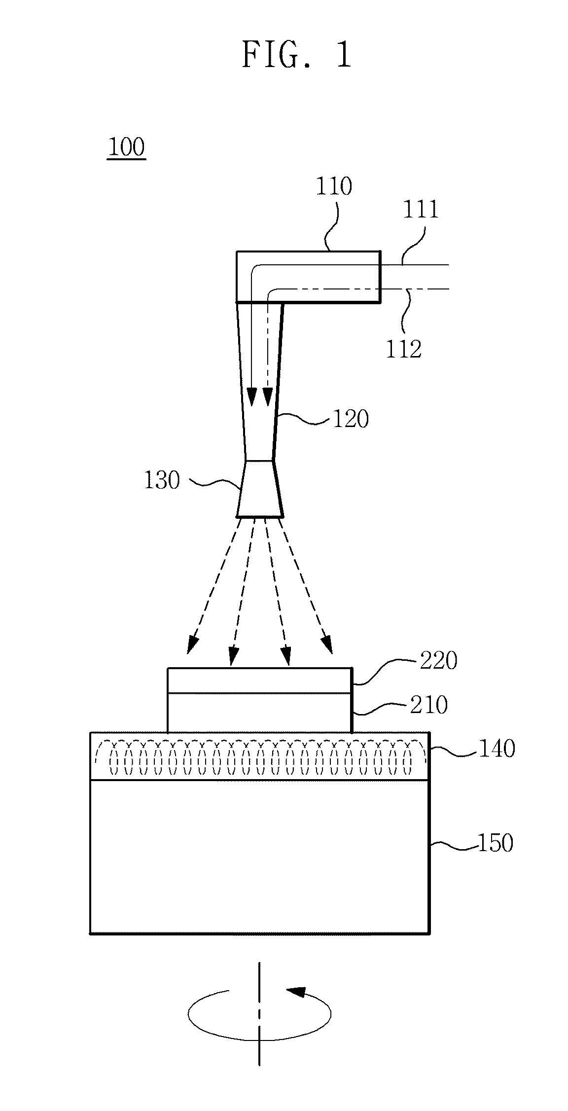
[0056]CuCl2, InCl3 and SeC(NH2)2 precursor solutions were blended in a nitrogen atmosphere so that as little contaminant as possible was added and then mixed at room temperature for about 5 min so that the reaction of respective reactants efficiently occurred, thus preparing a mixture solution represented by CuXInYSeZ (X=0.5˜1.4, Y=0.5˜1.4, Z=1˜6).

[0057]Formation of Thin Film

[0058]Nitrogen gas was controlled so as to be uniformly sprayed at 3˜50 ml / h on a Mo back contact layer heated at 300˜500° C. for 30˜60 min, and the substrate located under the Mo back contact layer was rotated at 10˜50 rpm, whereby the mixture solution was sprayed thereon, and the thin film thus formed was dried by being slowly cooled to room temperature at a rate of 8˜12° C. / min, thus manufacturing a thin film 1 μm thick.

[0059]Selenization

[0060]The thin film was selenized in a Se atmosphere at 450˜610° C. for 30˜120 min,...

example 2

Formation of CIGS-Based Thin-Film Light-Absorbing Layer

[0061]A thin-film light-absorbing layer was manufactured in the same manner as in Example 1, with the exception that GaCl3 was further added to the mixture solution so that the mixture solution contained Ga which replaces some percentage (20%) of In.

example 3

Fabrication of CIS-Based Thin-Film Solar Cell

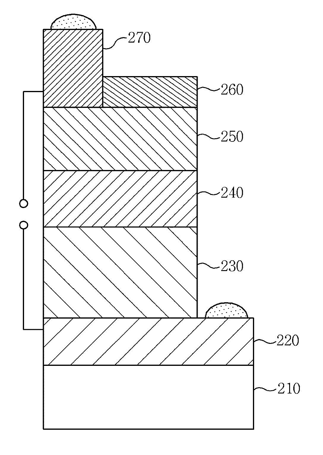
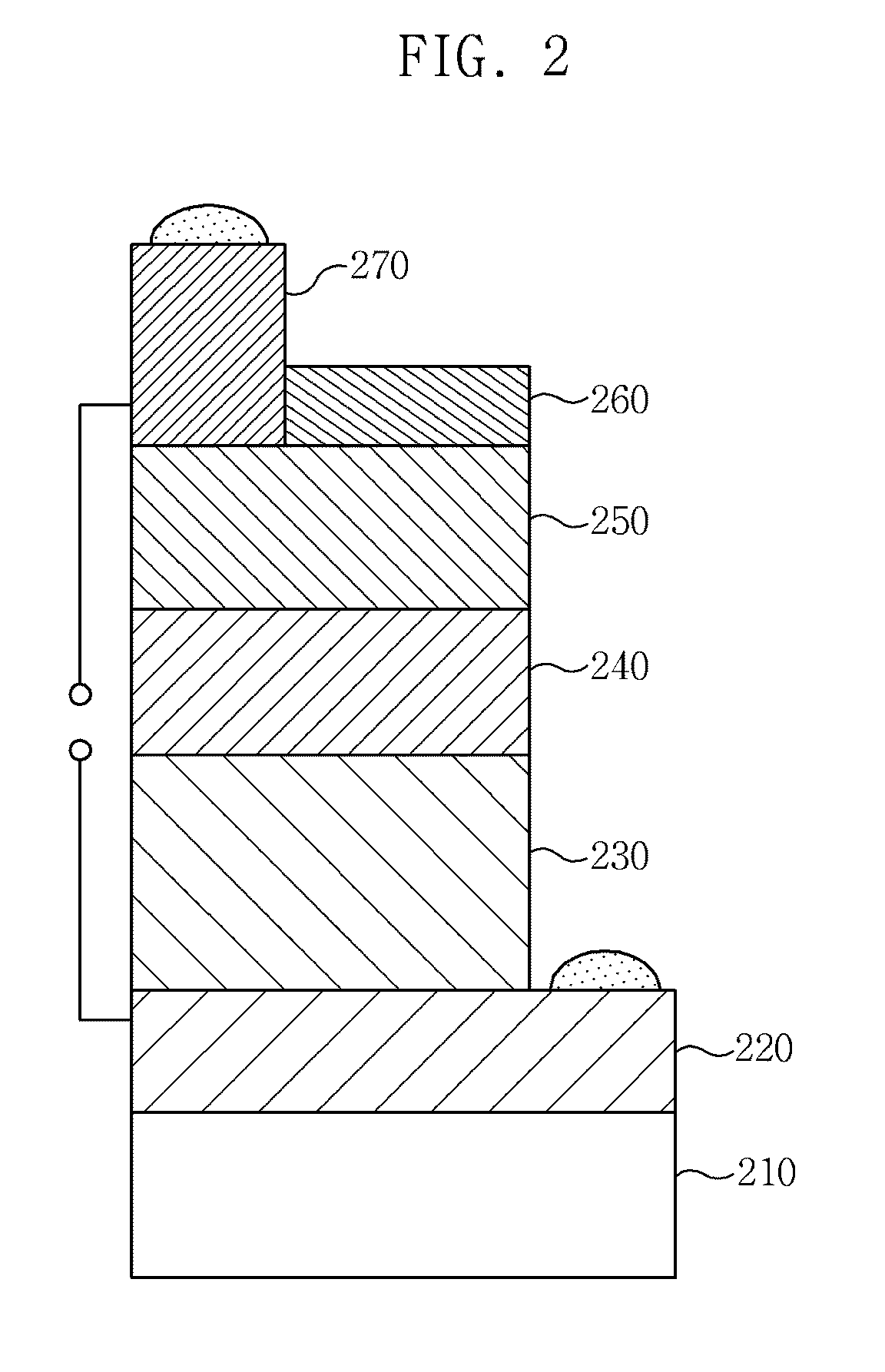
[0062]Formation of Back Contact Layer

[0063]Mo was deposited to a thickness of 1 μm on a glass substrate or a sodalime glass substrate using sputtering, thus forming a Mo back contact layer.

[0064]Formation of CIS-Based Light-Absorbing Layer

[0065]The CIS-based thin-film light-absorbing layer was formed to a thickness of 1 μm using the procedures of Example 1.

[0066]Formation of Buffer Layer

[0067]A CdS buffer layer was formed on the light-absorbing layer using chemical vapor deposition.

[0068]Formation of Window Layer

[0069]On the buffer layer, i-ZnO and n-ZnO were sequentially deposited using sputtering, thus forming a window layer.

[0070]Formation of Upper Electrode Layer

[0071]An Al upper electrode layer was formed to a thickness of 1 μm on the window layer using sputtering, thereby manufacturing a CIS-based thin-film solar cell.


PUM

PropertyMeasurementUnit
thicknessaaaaaaaaaa
energy gapaaaaaaaaaa
temperatureaaaaaaaaaa

Abstract

Disclosed is a method of manufacturing a thin-film light-absorbing layer using spraying, including mixing precursor solutions comprising CuCl2, InCl3 and SeC(NH2)2 under a nitrogen atmosphere at room temperature thus preparing a mixture solution; spraying the mixture solution on a substrate and drying it, thus forming a thin film; and selenizing the thin film under a selenium atmosphere. A method of manufacturing a thin-film solar cell is also provided, which includes forming a back contact layer on a glass substrate using sputtering; forming a light-absorbing layer on the back contact layer using spraying; forming a buffer layer on the light-absorbing layer using chemical vapor deposition; forming a window layer on the buffer layer using sputtering; and forming an upper electrode layer on the window layer.

Description

CROSS REFERENCE TO RELATED APPLICATIONS[0001]This application claims the benefit of Korean Patent Application Nos. 10-2010-0018121, filed Feb. 26, 2010 and 10-2010-0081632, filed Aug. 23, 2010, which are hereby incorporated by reference in their entirety into this application.BACKGROUND OF THE INVENTION[0002]1. Technical Field[0003]The present invention relates to a method of manufacturing a thin-film light-absorbing layer and a method of manufacturing a thin-film solar cell using the same.[0004]2. Description of the Related Art[0005]Materials for use in thin-film solar cells include crystalline silicon, amorphous silicon, a dye sensitizer, CIS, CIGS, CdTe, etc. Among these materials, a CIS-based compound which shows the highest theoretical efficiency is useful in the fabrication of solar cells. Currently, a CIS-based thin-film light-absorbing layer is being manufactured using a high-vacuum apparatus via co-evaporation or sputtering. As is known to date, the light conversion efficie...

Claims


Application Information

Patent Timeline
Patent Type & Authority Patents(United States)
IPC IPC(8): H01L21/00H01L31/0749
CPCH01L21/02422H01L21/02491H01L21/02568H01L21/02614H01L31/022466H01L31/0322H01L31/0749H01L21/02628Y02E10/541Y02P70/50
Inventor CHO, JUNG-MINBAE, EUN-JINHAM, CHANG-WOOSUH, JEONG-DAECHUNG, MYUNG-AESONG, KI-BONG
Owner ELECTRONICS & TELECOMM RES INST
Why Eureka
Try Eureka